
User Guide


User Guide
iolinker Evaluation Board JI11x-81L-B
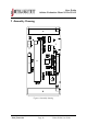
3 Special GPIOs
These pins are normal GPIOs, but in the iolinker application hold special meaning.
3.1 Enable
The EN pin is a pullup in the iolinker application. With a jumper it can be connected to
GND on the board to activate the GPIOs P1 - P49. As P1 - P49 is open collector otherwise,
this can also be used for multiplexing.
3.2 Interrupt
The INT pin is defined as an open collector pin with external pullup, that can be connected
in parallel between multiple boards. The iolinker application notifies about input pin changes
with a 10ms low signal on this pin.
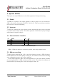
3.3 Communication interface
Pin UART SPI I2C
COM1 – CLK Clock
COM2 RX MOSI –
COM3 TX (open collector when idle) MISO Data
COM4 – SS –
Table 3: Communication pins
COM1 - COM3 can always be connected in parallel, when using multiple boards.
3.4 Address encoding
The 0K resistors marked as IN1 - IN7 on the front silkscreen connect to GND. When the
FPGA software uses an internal pullup on those pins, the resistors can be used for encoding
static configuration options, such as slave addresses.
In the iolinker application, IN1 is the least significant bit of the slave address, and IN7
the most significant bit. A GND connection encodes a 0 bit. The default slave addresses is
therefore 0x00. By removing IN1, it could be changed to 0x01, etc.
c
2017 jInvent. The specifications and information herein are subject to change without notice.
www.jinvent.de Page 5 iolinker Board User Guide