User Guide iolinker Evaluation Board JI11x-81L-B
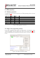
User Guide iolinker Evaluation Board JI11x-81L-B 1 Features Figure 1: Product illustration The evaluation board for the JI11x-81L chips is a Lattice MachXO3 FPGA board with 49 GPIOs. FPGA Supply voltage VCC_IO VCC_core JTAG port GPIO list LCMXO3L-4300E-5UWG81CTR50 3.3 V – 5 V, MicroUSB for power supply available 3.3 V with internal voltage regulator, can be manually changed to 1.2 V – 3.465 V 1.
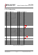
User Guide iolinker Evaluation Board JI11x-81L-B 2 Pin Configurations Pin A1 A2 A3 A4 A5 A6 A7 A8 A9 B1 B2 B3 B4 B5 Designation GND IN1 IN2 VCCIO IN3 IN4 P1 P2 GND P3 P4 P5 P6 P7 Function – Slave address[0] LSB Slave address[1] – Slave address[2] Slave address[3] GPIO / TDI GPIO / Push button – GPIO / DONE GPIO / LED GPIO / LED GPIO GPIO Pin E6 E7 E8 E9 F1 F2 F3 F4 F5 F6 F7 F8 F9 G1 Designation P22 P23 P24 VCC P25 P26 VCC P27 P28 P29 P30 P31 VCCIO COM4 B6 B7 B8 B9 C1 C2 C3 C4 C5 CLK P8 IN5 IN6 P9 P10
User Guide iolinker Evaluation Board JI11x-81L-B Pin Designation Function Pin Designation Function D2 JTAGEN Use 10k pull-down to H7 COM1 NC1 , GND SPI CLK2 , I2C SCL3 D3 P11 GPIO H8 P43 GPIO D4 P12 / TMS GPIO H9 P44 GPIO D5 P13 GPIO J1 GND – D6 P14 GPIO J2 P45 GPIO D7 P15 GPIO J3 P46 GPIO D8 P16 GPIO J4 VCCIO – D9 P17 GPIO J5 P47 GPIO E1 P18 GPIO J6 P48 GPIO E2 P19 GPIO J7 COM3 UART TX1 , SPI MISO2 , I2C Data3 E3 P20 GPIO J8 P49 GPIO E4 P21 GPIO / TCK J9 GND – E5 GND – Table 2: Pin description WLCSP-81 Ta
User Guide iolinker Evaluation Board JI11x-81L-B 3 Special GPIOs These pins are normal GPIOs, but in the iolinker application hold special meaning. 3.1 Enable The EN pin is a pullup in the iolinker application. With a jumper it can be connected to GND on the board to activate the GPIOs P1 - P49. As P1 - P49 is open collector otherwise, this can also be used for multiplexing. 3.
User Guide iolinker Evaluation Board JI11x-81L-B 4 Changing VCC_IO If you intend to change VCC_IO to another voltage than the 3.3 V used by default, remove resistors R71 and R75. Then connect at least one pad (near the FPGA) to another voltage between 1.2 V and 3.465 V. On the connector X7, pin 20 is unused and can be repurposed. Take care to not damage the FPGA when soldering. After changing VCC_IO, the input and output voltage level of all GPIOs will change. This includes the JTAG interface.
User Guide iolinker Evaluation Board JI11x-81L-B 5 JTAG interface 5.1 Hardware preparation To program the FPGA, connect the pins from your JTAG programming cable to the board as listed in table 4. JTAG cable pin TDI TDO TMS TCK GND PROG VCC INIT TRST Board pin TDI TDO TMS TCK GND JTAGEN VCC_IO – – Header X2 X2 X2 X2 X2 X2 X5, X6 or X7 – – Table 4: JTAG programmer connections 5.2 Usage of the programming software In the Lattice Programmer utility, create a new blank project.
User Guide iolinker Evaluation Board JI11x-81L-B Click the "JTAG Scan" button. The FPGA should be recognized and identified automatically. If it fails, don’t forget to verify that the just made "Custom I/O settings" are still in effect before retrying. Choose "Erase, Program, Verify" as operation and select a *.jed file. You can now click "Program" to transfer your new application onto the board. Be careful: NVCM programming can only be done 9 times.
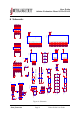
5 X5 A4 C5 C7 G6 J4 U5A BANK0 VCCIO VCCIO VCCIO JI111-81L U5B BANK2 VCCIO VCCIO JI111-81L VCCIO VCC_int VCCIO VCC_int 4 P13 EN P2 IN5 P8 P1 P21 P12 IN4 CLK P20 P11 IN3 P7 IN7 P6 P26 P19 CTRL P10 P5 IN2 P25 P18 IN1 P4 P9 P3 P15 P14 P48 P42 P41 P47 P34 P40 P33 P32 P39 P46 P38 P45 COM4 COM2 P44 P49 P43 P35 COM1 COM3 D5 C6 A8 B8 B7 A7 E4 D4 A6 B6 E3 D3 A5 B5 C3 B4 F2 E2 D2 C2 B3 A3 F1 E1 A2 B2 C1 B1 D7 D6 J6 H6 H5 J5 G4 H4 G3 G2 H3 J3 H2 J2 G1 H1 H9 J8 H8 G7 H7 J7 P48 P42 P41 P47 P34 P40 P33 P
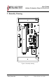
User Guide iolinker Evaluation Board JI11x-81L-B 7 Assembly Drawing Figure 4: Assembly drawing c 2017 jInvent. The specifications and information herein are subject to change without notice. www.jinvent.
User Guide iolinker Evaluation Board JI11x-81L-B Contents 1 Features 2 2 Pin Configurations 3 3 Special GPIOs 3.1 Enable . . . . . . . . . . 3.2 Interrupt . . . . . . . . . 3.3 Communication interface 3.4 Address encoding . . . . . . . . . . . . . . . . . . . . . . . . . . . . . . . . . . . . . . . . . . . . . . . . . . . . . . . . . . . . . . . . . . . . . . . . . . . . . . . . . . . . . . . . . . . . . . . . . . . . . . . . . . . . . . . . .