
Data Sheet

iolinker Family Data Sheet
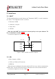
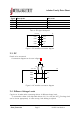
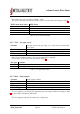
Signal Description Idle state
SCLK Synchronous clock from the master to slaves High
MOSI Input line to the slaves from the master High
MISO Output line from the slaves to the master Tristate
SS Slave select High
Table 1: SPI signal description
COM2
COM3
uCJ112−100
COM4
COM1
SCLK
MOSI
MISO
SS
Figure 2: SPI interface connection diagram
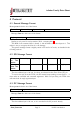
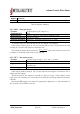
2.3 I2C
Details to be announced.
A connection diagram can be seen in figure 3.
COM2
COM3
uCJ113−100
COM4
COM1
SCL
SDA
Vcc
RpRp
Figure 3: I2C interface connection diagram
2.4 Different Voltage Levels
Care has to be taken when connecting devices of different voltage levels.
To connect the iolinker 1.2V chips with devices of 3.3 V or less, the VCC_IO voltage level
can be chosen appropriately. In other set-ups, level shifting is required.
c
2017 jInvent. The specifications and information herein are subject to change without notice.
www.jinvent.de Page 5 iolinker introduction