
Data Sheet

iolinker Family Data Sheet
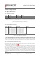
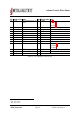
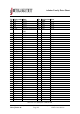
Name Pin type Function Note
COM2 Input UART Receive Only available in iolinker
UART version
COM3 Open collector output, exter-
nal pull-up required
UART Transmit
COM1 Input SPI Clock
COM2 Input SPI MOSI Only available in iolinker SPI
version
COM3 Output SPI MISO
COM4 Input SPI Slave Select
COM1 Input I2C Clock Only available in iolinker I2C
version
COM3 Open Collector Output I2C Data
Table 19: Communication pin description
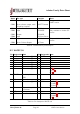
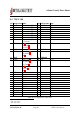
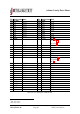
9.2 WLCSP-36
Pin Designation Note Pin Designation Note
A1 IN1 Slave address[0] LSB D1 GND –
A2 IN2 Slave address[1] D2 P5 GPIO
A3 VCCIO0 – D3 P6 GPIO
A4 IN3 Slave address[2] D4 P7 GPIO
A5 IN4 Slave address[3] D5 VCC –
A6 IN5 Slave address[4] D6 P8 GPIO
B1 IN6 Slave address[5] E1 COM4 NC
1
,
SPI SS
2
,
NC
3
B2 JTAGEN Use 10k pull-down to
GND
E2 P9 GPIO
B3 CLK Optional E3 P10 GPIO
B4 IN7 Slave address[6] MSB E4 COM3 UART TX
1
,
SPI MISO
2
,
I2C Data
3
B5 EN Chip enable, pull low
to activate
E5 P11 GPIO
B6 INT Interrupt output E6 P12 GPIO
C1 VCC – F1 COM2 UART RX
1
,
SPI MOSI
2
,
NC
3
Table 20: Pin description WLCSP-36
c
2017 jInvent. The specifications and information herein are subject to change without notice.
www.jinvent.de Page 22 iolinker introduction