iolinker Family Data Sheet
iolinker Family Data Sheet 1 Introduction 1.1 Features • IO extension with synchronized pin updates • Dynamic IO matrix connections for signals up to 29.
iolinker Family Data Sheet • PWM controller, e.g. for huge LED panels • Frequency generation c 2017 jInvent. The specifications and information herein are subject to change without notice. www.jinvent.
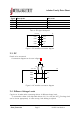
iolinker Family Data Sheet 2 Interfaces 2.1 UART The Universal Asynchronous serial Receiver and Transmitter (UART) is a serial communication device. The configuration used is as follows: • Baud rate: 115200 • 8 data bits, 1 stop bit • Parity: None • LSB first Note that this UART bus requires an external pull-up on its open collector TX line, as described in section 9.1.3. A connection diagram can be seen in figure 1.
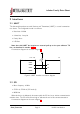
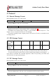
iolinker Family Data Sheet Signal SCLK MOSI MISO SS Description Synchronous clock from the master to slaves Input line to the slaves from the master Output line from the slaves to the master Slave select Idle state High High Tristate High Table 1: SPI signal description J112−100 uC COM1 SCLK COM2 MOSI COM3 MISO COM4 SS Figure 2: SPI interface connection diagram 2.3 I2C Details to be announced. A connection diagram can be seen in figure 3.
iolinker Family Data Sheet 3 Timing 3.1 SPI Protocol When writing out an SPI command that requires a reply from the FPGA, the master has to keep writing out n + 1 zero bytes, where n is the number of bytes to be read back. This means that with one byte delay, the FPGA will begin sending out its response bytes. 3.2 Interrupt Pin The interrupt pin INT notifies about state change of any GPIO currently configured as input.
iolinker Family Data Sheet 4 Protocol 4.1 General Message Format Messages to the device are of the format Slave address Command byte Argument bytes Messages from the device are of the format Reply argument bytes Replies are only sent for read operations (W=1, compare table 2). The MSB of the command byte is always 1, and the MSB of all other bytes is 0. This makes it easy to recognize the start of a new message.
iolinker Family Data Sheet 4.4 Command Destination Address The target address byte of the format 0sss ssss allows to target specific slave devices with a command. Each device processes messages only when addressed correctly with its userdefined slave address. The slave address can be configured through the hardware address pins as described in section 9.1.2. The target address 0x7f holds a special function in the protocol, for it is always executed, regardless of the actual slave address.
iolinker Family Data Sheet The version byte can hold values of 0x00 – 0x7f. The GPIO count byte encodes the GPIO count in its lower nibble according to table 4. GPIO count byte value 0x0 0x1 0x2 0x3 GPIO count 14 49 64 192 Table 4: GPIO count encoding 4.7.
iolinker Family Data Sheet Address 0x7f Function Status register Table 6: Register addresses 4.7.4 REA – Read pin states Function Command byte Argument list Reply argument list Example arguments Read the state of pin range x to y 0xC7 First pin address to read, last pin address to read Current pin states 0x01 0x00 | 0x7f 0x00 (Read pins P1 to P127 ) To read pin states, use the first and the last pin address as parameters. If the last pin number equals 0, only one pin state will be read.
iolinker Family Data Sheet 4.7.6 SYN – Synchronize Buffered IO State Function Command byte Argument list Enable command buffering 0x88 – Use this command before you start issuing write commands you want to buffer. To end the buffer process, issue a TRG command. 4.7.7 TRG – Trigger IO State Buffer Execution Function Command byte Argument list Execute all buffered IO states (i.e. copy buffer to current and write out pin states) 0x89 – Use this command to write out the buffered IO states, i.e.
iolinker Family Data Sheet The PWM_R argument byte has the format 0rrr rrrr, i.e. there are 128 possible values between 0 and 127, as seen in table 7. PWM_R byte value 0x00 0x01 ... 0x3f 0x40 ... 0x7f PWM ratio 0:127 1:127 ... 63:127 64:127 ... 127:127 PWM ratio in % 0% 0.8% ... 49.6% 50.4% ... 100% Table 7: PWM_R byte values and their meaning Note that the output state needs to be high for PWM output to be active. To turn PWM off, set the PWM ratio to 100%. 4.7.
iolinker Family Data Sheet 5 Pin Addresses Pin addresses are encoded in two bytes of the format 0PPPPPPP 00000PPP, where the first byte encodes the less significant 7 bits of the pin number, and the second byte encodes the more significant bits of the pin number. On devices with less than 128 pins, the second byte is always 0x00. The second byte for pin numbers below 128 is therefore 0x00. Examples for physical pin addresses are listed in table 8.
iolinker Family Data Sheet 6 Default Pin States Pin P1 P2 P3 P4 P5 P6 – P49 Default state Output, pull down Input Output, pull down Output, linked to P2 Output, low Output, pull down Table 9: Default pin states c 2017 jInvent. The specifications and information herein are subject to change without notice. www.jinvent.
iolinker Family Data Sheet 7 Application Notes 7.
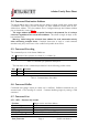
iolinker Family Data Sheet 7.2 Basic schematic for WLCSP-81 See JI11x-81L-B User Guide. 7.3 High Power LED Example P2 R59 100 G Using MOSFETs, the iolinker device can be used to control high power LEDs and entire LED panels. P2 VCC3V3 D S K1 AO3401 R60 100 HIPWR LED Figure 5: High power LED controller c 2017 jInvent. The specifications and information herein are subject to change without notice. www.jinvent.
iolinker Family Data Sheet 8 Electrical Characteristics 8.1 Recommended Operating Conditions Symbol VCC VCCAUX VCCIO tJCOM Parameter Core Supply Voltage for 3.3V chips Auxiliary Supply Voltage I/O Driver Supply Voltage Junction Temperature Min. 1.71 3.135 1.14 0 Max. Units 3.465 V 3.465 V 3.465 V +85 ◦C Table 10: Recommended Operating Conditions of 3.3V chips Symbol Parameter Core Supply Voltage for 1.2 V Devices VCC Core Supply Voltage for 2.5 V/3.
iolinker Family Data Sheet 8.2 Absolute Maximum Ratings Parameter Supply Voltage VCC Supply Voltage VCCAUX Output Supply Voltage I/O Tristate Voltage Applied Dedicated Input Voltage Applied Storage Temperature (ambient) Junction Temp. (Tj ) 3.3V chips −0.5 to 3.75 V −0.5 to 3.75 V −0.5 to 3.75 V −0.5 to 3.75 V −0.5 to 4.25 V −65 to 150 ◦C +125 ◦C Table 12: Absolute Maximum Ratings of 3.
iolinker Family Data Sheet 8.3 Typical DC Characteristics Symbol IIL , IIH IPU IPD IBHLS IBHHS IBHLO IBHHO VBHT C1 C2 Parameter Condition Min. Typ. Max. Units 0 ≤ VIN ≤ (VCCIO − 0.2 V) — — 10 µA Input or I/O Leakage (VCCIO − 0.2 V) < VIN ≤ 3.6 V — — 40 µA I/O Active Pull-up Current 0 ≤ VIN ≤ 0.7VCCIO −30 — −150 µA I/O Active Pull-down Current VIL (MAX) ≤ VIN ≤ VIH (MAX) 30 — 150 µA Bus Hold Low Sustaining current VIN = VIL (MAX) 30 — — µA Bus Hold Low Overdrive current VIN = 0.
iolinker Family Data Sheet 8.4 Single-Ended DC Electrical Characteristics Input/Output Standard LVCMOS3.3 (3.3 V chips) LVCMOS1.2 (1.2 V chips) Min. (V) −0.3 VIL Max. (V) 0.8 VIH VOL Max. VOH Min. Min. Max. (V) (V) (V) (V) 2.0 3.6 −0.3 0.35VCCIO 0.65VCCIO 3.6 0.4 VCCIO − 0.4 0.2 VCCIO − 0.2 0.4 VCCIO − 0.4 0.2 VCCIO − 0.2 IOL (mA) IOH (mA) 4 8 12 16 0.1 4 8 0.1 −4 −8 −12 −16 −0.1 −2 −6 −0.1 Table 16: DC Electrical Characteristics of Single-Ended GPIOs c 2017 jInvent.
iolinker Family Data Sheet 9 Pin Configurations 9.1 Signal Descriptions 9.1.1 General Pin Listing Name EN INT Pin type Input Open collector output Function Chip enable∗ Interrupt pin∗∗ Note Pull low to activate chip Use external pull-up ∗ When the chip is not enabled, all outputs are in their default state, pin links are inactive and no communication is processed. ∗∗ Informs about updates of input GPIOs, multiple devices can be connected on a single interrupt bus line.
iolinker Family Data Sheet Name COM2 Pin type Input Function UART Receive COM3 UART Transmit COM1 COM2 Open collector output, external pull-up required Input Input COM3 COM4 COM1 Output Input Input SPI MISO SPI Slave Select I2C Clock COM3 Open Collector Output I2C Data SPI Clock SPI MOSI Note Only available in iolinker UART version Only available in iolinker SPI version Only available in iolinker I2C version Table 19: Communication pin description 9.
iolinker Family Data Sheet Pin C2 C3 C4 C5 Designation P1 P2 P3 GND C6 P4 Note GPIO GPIO GPIO – Pin F2 F3 F4 F5 Designation VCCIO P13 P14 COM1 GPIO F6 VCCIO Note – GPIO GPIO NC1 , SPI CLK2 , I2C SCL3 – Table 20: Pin description WLCSP-36 1 UART chip version 2 SPI chip version 3 I2C chip version c 2017 jInvent. The specifications and information herein are subject to change without notice. www.jinvent.
iolinker Family Data Sheet 9.
iolinker Family Data Sheet Pin Designation Note Pin Designation Note D2 CTRL Use 10k pull-down to H7 COM1 NC4 , GND SPI CLK5 , I2C SCL6 D3 P11 GPIO H8 P43 GPIO D4 P12 / TMS GPIO H9 P44 GPIO D5 P13 GPIO J1 GND – D6 P14 GPIO J2 P45 GPIO D7 P15 GPIO J3 P46 GPIO D8 P16 GPIO J4 VCCIO – D9 P17 GPIO J5 P47 GPIO E1 P18 GPIO J6 P48 GPIO E2 P19 GPIO J7 COM3 UART TX4 , SPI MISO5 , I2C Data6 E3 P20 GPIO J8 P49 GPIO E4 P21 GPIO / TCK J9 GND – E5 GND – Table 21: Pin description WLCSP-81 4 UART chip version 5 SPI chip v
iolinker Family Data Sheet 9.
iolinker Family Data Sheet Pin 27 28 29 30 31 32 33 34 35 36 37 38 39 40 41 42 43 44 45 46 47 48 Designation P9 NC P10 P11 NC P12 NC P13 VCC P14 P15 CLK P16 GND VCCIO1 GNDIO1 P17 P18 P19 P20 P21 SLEEP 49 P22 50 P23 Note GPIO – GPIO GPIO – GPIO – GPIO – GPIO GPIO Optional GPIO – – – GPIO GPIO GPIO GPIO GPIO Use 10k pull-up to VCC_3V3 GPIO GPIO Pin 77 78 79 80 81 82 83 84 85 86 87 88 89 90 91 92 93 94 95 96 97 98 Designation P46 P47 P48 P49 P50 P51 P52 GND P53 P54 P55 VCCAUX P56 VCC P57 VCCIO0 GNDIO0 P5
iolinker Family Data Sheet 9.
iolinker Family Data Sheet Pin C6 C7 C8 C9 C10 Designation P22 P23 P24 P25 CTRL C11 C12 C13 C14 C15 C16 D1 D2 D3 D4 D5 D6 D7 D8 D9 D10 D11 D12 D13 D14 D15 D16 E1 E2 E3 E4 E5 E6 E7 E8 E9 E10 E11 E12 P26 P27 P28 GND P29 P30 P31 P32 P33 GND VCCIO P34 P35 P36 P37 P38 P39 VCCIO GND P40 P41 P42 P43 P44 P45 VCCIO GND P46 P47 P48 P49 P50 P51 GND Note Pin Designation GPIO L6 GND GPIO L7 P122 GPIO L8 P123 GPIO L9 P124 Use 10k pull-down to L10 P125 GND GPIO L11 GND GPIO L12 P126 GPIO L13 P127 – L14 P128 GPIO L15
iolinker Family Data Sheet Pin E13 E14 E15 E16 F1 F2 F3 F4 F5 F6 Designation VCCIO P52 P53 P54 P55 P56 P57 P58 P59 GND Note – GPIO GPIO GPIO GPIO GPIO GPIO GPIO GPIO – Pin N13 N14 N15 N16 P1 P2 P3 P4 P5 P6 Designation GND P152 P153 P154 P155 P156 GND P157 P158 COM1 F7 F8 F9 F10 F11 F12 F13 P60 P61 P62 P63 GND P64 P65 GPIO GPIO GPIO GPIO – GPIO GPIO P7 P8 P9 P10 P11 P12 P13 P159 P160 P161 P162 P163 P164 COM2 F14 F15 F16 G1 G2 G3 G4 G5 G6 G7 G8 G9 G10 G11 P66 P67 P68 P69 P70 P71 P72 P73 P74 VCC VC
iolinker Family Data Sheet Pin Designation Note G12 P76 GPIO G13 G14 G15 G16 H1 H2 H3 H4 H5 H6 P77 P78 P79 P80 P81 P82 P83 P84 P85 P86 GPIO GPIO GPIO GPIO GPIO GPIO GPIO GPIO GPIO GPIO H7 H8 H9 H10 H11 H12 H13 H14 H15 H16 VCCIO GND GND VCCIO P87 P88 P89 P90 P91 P92 – – – – GPIO GPIO GPIO GPIO GPIO GPIO Pin Designation Note R12 COM4 NC10 , SPI SS11 , NC12 R13 P177 GPIO R14 P178 GPIO R15 GND – R16 P179 GPIO T1 VCC – T2 P181 GPIO T3 P182 GPIO T4 P183 GPIO T5 P184 GPIO T6 COM3 UART TX10 , SPI MISO11 , I
iolinker Family Data Sheet 10 Ordering Information Ordering Code JI107-100 JI108-100 JI109-100 JI111-36L JI112-36L JI113-36L JI114-36L JI115-36L JI116-36L JI111-81L JI112-81L JI113-81L JI114-81L JI115-81L JI116-81L JI117-256 JI118-256 JI119-256 Package TQFP-100 TQFP-100 TQFP-100 WLCSP-36 WLCSP-36 WLCSP-36 WLCSP-36 WLCSP-36 WLCSP-36 WLCSP-81 WLCSP-81 WLCSP-81 WLCSP-81 WLCSP-81 WLCSP-81 CABGA-256 CABGA-256 CABGA-256 Pin count 100 100 100 36 36 36 36 36 36 81 81 81 81 81 81 256 256 256 GPIO 60 60 60 14 14
iolinker Family Data Sheet 11 Packaging Information Package WLCSP-36 WLCSP-81 TQFP-100 CABGA-256 Spacing 0.4 mm 0.4 mm 0.5 mm 0.8 mm Size 2.5 × 2.5 mm 3.8 × 3.8 mm 14 × 14 mm 14 × 14 mm Table 25: Packaging information for chip models c 2017 jInvent. The specifications and information herein are subject to change without notice. www.jinvent.
iolinker Family Data Sheet 12 Errata The revision letter in this section refers to the revision of the iolinker device. 12.1 iolinker Rev. A Initial release. c 2017 jInvent. The specifications and information herein are subject to change without notice. www.jinvent.
iolinker Family Data Sheet 13 Revision History Date September 2016 December 2016 January 2017 January 2017 March 2017 April 2017 Version 1 2 3 4 5 6 Section – – – – – – Change Summary Initial release. Revised datasheet to match new products. Corrected pin listing for WLCSP-81. Corrected argument listing for TYP command.
iolinker Family Data Sheet Contents 1 Introduction 1.1 Features . . . . . . . . . . . . . . . . . . . . . . . . . . . . . . . . . . . . 1.2 Introduction . . . . . . . . . . . . . . . . . . . . . . . . . . . . . . . . . . 1.3 Applications . . . . . . . . . . . . . . . . . . . . . . . . . . . . . . . . . . 2 2 2 2 2 Interfaces 2.1 UART . . . . . 2.2 SPI . . . . . . . 2.3 I2C . . . . . . . 2.4 Different Voltage . . . . 4 4 4 5 5 3 Timing 3.1 SPI Protocol . . . . . . . . . . . . . . . . . . . . . . . . .
iolinker Family Data Sheet 8 Electrical Characteristics 8.1 Recommended Operating Conditions . . . 8.2 Absolute Maximum Ratings . . . . . . . . 8.3 Typical DC Characteristics . . . . . . . . . 8.4 Single-Ended DC Electrical Characteristics . . . . . . . . . . . . . . . . . . . . . . . . . . . . . . . . . . . . . . . . . . . . . . . . . . . . . . . . . . . . . . . . . . . . . . . . 17 17 18 19 20 9 Pin Configurations 9.1 Signal Descriptions . . . . . . . . . . . . . . 9.1.