
User's Manual


Host Board Design
A DIVISION OF TRIMBLE
Hardware Integration 51
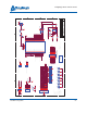
module pad positional tolerance shall be not more than +/-0.2 mm to support contact
alignment during fixturing.
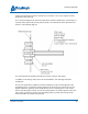
The circuitry feeding the RF pad of the M6e-Nano shall be optimized for connecting to a
coplanar wave guide with ground plane beneath. The CPW-G will have dimensions as
shown in the following diagram.
The area beneath the module should be kept clear of traces and copper.
In addition to the design and process recommendations, the following should be
considered:
There is the potential for 24MHz harmonics radiating from pins 22 through 28 of the
ThingMagic Nano. If emissions testing shows such harmonics the easiest fix is to put
bypass capacitors (typically 39 to 100pf) directly at the ¬offending pins on the carrier
board. Note that higher values are not necessarily better. The ideal capacitor value will
have series resonance near the most offending frequency. 39pF has been good for
around 900 MHz in sample board layouts.