
Datasheet


© 2006 IXYS All rights reserved
2 - 3
0639
CS 45
IXYS reserves the right to change limits, test conditions and dimensions.
Symbol Conditions Characteristic Values
min. max.
I
R
, I
D
V
R
= V
RRM
; V
D
= V
DRM
; T
VJ
= T
VJM
5 mA
V
T
I
T
= 80 A; T
VJ
= 25°C 1.64 V
V
TO
r
T
For power-loss calculations only
T
VJ
= 125°C
0.85
11
V
mW
V
GT
I
GT
V
D
= 6 V; T
VJ
= 25°C
T
VJ
= -40°C
V
D
= 6 V; T
VJ
= 25°C
T
VJ
= -40°C
1.5
1.6
100
200
V
V
mA
mA
V
GD
I
GD
V
D
=
2
/
3
V
DRM
; T
VJ
= T
VJM
0.2
10
V
mA
I
L
t
p
= 10 µs; T
VJ
= 25°C
I
G
= 0.3 A; di
G
/dt = 0.3 A/µs
150 mA
I
H
V
D
= 6 V; R
GK
= ∞; T
VJ
= 25°C 100 mA
t
gd
V
D
= ½ V
DRM;
T
VJ
= 25°C
I
G
= 0.3 A; di
G
/dt = 0.3 A/µs
2 µs
R
thJC
R
thJH
DC current
DC current
0.62
0.82
K/W
K/W
a
Max. acceleration; 50 Hz 50 m/s
2
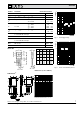
TO-247 AD
Dim.
Millimeter Inches
Min. Max. Min. Max.
A 19.81 20.32 0.780 0.800
B 20.80 21.46 0.819 0.845
C 15.75 16.26 0.610 0.640
D 3.55 3.65 0.140 0.144
E 4.32 5.49 0.170 0.216
F 5.40 6.20 0.212 0.244
G 1.65 2.13 0.065 0.084
H - 4.50 - 0.177
J 1.00 1.40 0.040 0.055
K 10.80 11.00 0.426 0.433
L 4.70 5.30 0.185 0.209
M 0.40 0.80 0.016 0.031
N 1.50 2.49 0.087 0.102
Dimensions (1 mm = 0.0394")
The convex bow of substrate is typ. < 0.04 mm over plastic surface level
of device bottom side
This drawing will meet all dimensions requirement of JEDEC outline
TO-247 AD except screw hole and except Lmax.
ISOPLUS 247
TM
10 100 1000
1
10
100
1000
Ps
t
gd
I
G
1 10 100 1000 10000
0.1
1
10
I
G
V
G
mA
V
4
2
1
5
6
mA
typ.
Limit
3
Fig. 1 Gate trigger range
Fig. 2 Gate controlled delay time t
gd