
Data Sheet

Page 79
nRF51822 Product Specification v3.1
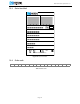
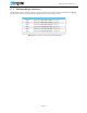
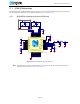
11.3 QFAA QFN48 package
Documentation for the QFAA QFN48 package reference circuit, including Altium Designer files, PCB layout
files, and PCB production files can be downloaded from www.nordicsemi.com.
11.3.1 QFAA QFN48 schematic with internal LDO setup
Figure 22 QFAA QFN48 with internal LDO setup
Note: For PCB reference layouts, see the Reference Layout section on the Downloads tab for the
different chip variants on www.nordicsemi.com.
C1
12pF
C2
12pF
X1
16MHz
C9
1.0nF
C8
100nF
C10
47nF
C11
100nF
VCC_nRF
VCC_nRF
GND
VCC_nRF
C7
100nF
P0.07
P0.30
P0.08
P0.09
P0.10
P0.11
P0.12
P0.13
P0.14
P0.15
P0.16
P0.17
P0.18
P0.19
P0.20
P0.21
P0.22
P0.23
P0.24
P0.25
P0.28
P0.29
P0.00
P0.01
P0.02
P0.03
P0.04
P0.06
SWCLK
SWDIO
P0.05
C3
2.2nF
C4
1.0pF
C5
2.2pF
C6
1.5pF
VDD
1
VDD
12
VSS
13
VDD_PA
30
ANT1
31
ANT2
32
VSS
33
VSS
34
AVDD
35
AVDD
36
XC1
37
XC2
38
nRF51x22
DCC
2
P0.30
3
P0.00
4
P0.01
5
P0.02
6
P0.03
7
P0.04
8
P0.05
9
P0.06
10
P0.07
11
P0.08
14
P0.09
15
P0.10
16
P0.11
17
DEC1
39
P0.21
40
P0.22
41
P0.23
42
P0.24
43
P0.25
44
P0.27
46
P0.26
45
P0.29
48
P0.28
47
P0.17
25
P0.18
26
P0.19
27
P0.20
28
DEC2
29
P0.12
18
P0.13
19
P0.14
20
P0.15
21
SWDIO/nRESET
23
SWDCLK
24
P0.16
22
U1
nRF51x22-QFAA
C14
12pF
C13
12pF
X2
32.768kHz
XL2
XL1
Optional
L1
4.7nH
L2
10nH
L3
3.3nH