
Data Sheet

Page 77
nRF51822 Product Specification v3.1
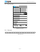
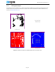
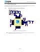
11.1.1 PCB layout example
The PCB layout shown in Figure 21 is a reference layout for the QFN package with internal LDO setup. For all
available reference layouts, see the Reference Layout section on the Downloads tab for the different chip
variants on www.nordicsemi.com.
Figure 21 PCB layout example for QFN48 package with internal LDO setup
Top silk screen
No components
in bottom layer
Top view Bottom view