
Data Sheet

Page 76
nRF51822 Product Specification v3.1
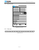
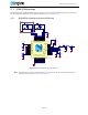
11 Reference circuitry
For the following reference layouts, C_pcb1 and C_pcb2, between X1 and XC1/XC2, is estimated to 0.5 pF
each.
The exposed center pad of the QFN48 package must be connected to supply ground for proper device
operation.
11.1 PCB guidelines
A well designed PCB is necessary to achieve good RF performance. A poor layout can lead to loss in
performance or functionality. A qualified RF layout for the IC and its surrounding components, including
matching networks, can be downloaded from www.nordicsemi.com.
To ensure optimal performance it is essential that you follow the schematics- and layout references closely.
Especially in the case of the antenna matching circuitry (components between device pins ANT1,ANT2,
VDD_PA and the antenna), any changes to the layout can change the behavior, resulting in degradation of
RF performance or a need to change component values. All the reference circuits are designed for use with a
50 ohm single end antenna.
A PCB with a minimum of two layers, including a ground plane, is recommended for optimal performance.
On PCBs with more than two layers, put a keep-out area on the inner layers directly below the antenna
matching circuitry (components between device pins
ANT1, ANT2, VDD_PA, and the antenna) to reduce the
stray capacitances that influence RF performance.
A matching network is needed between the differential RF pins
ANT1 and ANT2 and the antenna, to match
the antenna impedance (normally 50 ohm) to the optimum RF load impedance for the chip. For optimum
performance, the impedance for the matching network should be set as described in Section 8.5.7 “Antenna
matching network requirements” on page 54 along with the recommended QFN48 package reference
circuitry from Section 11.3 “QFAA QFN48 package” on page 79 and WLCSP package reference circuitry from
Section 11.7 “CEAA WLCSP package” on page 103.
The DC supply voltage should be decoupled as close as possible to the VDD pins with high performance RF
capacitors. See the schematics for recommended decoupling capacitor values. The supply voltage for the
chip should be filtered and routed separately from the supply voltages of any digital circuitry.
Long power supply lines on the PCB should be avoided. All device grounds, VDD connections, and VDD
bypass capacitors must be connected as close as possible to the IC. For a PCB with a topside RF ground
plane, the VSS pins should be connected directly to the ground plane. For a PCB with a bottom ground
plane, the best technique is to have via holes as close as possible to the VSS pads. A minimum of one via
hole should be used for each VSS pin.
Full-swing digital data or control signals should not be routed close to the crystal or the power supply lines.
Capacitive loading of full-swing digital output lines should be minimized in order to avoid radio
interference.