
Data Sheet

Page 60
nRF51822 Product Specification v3.1
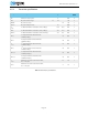
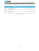
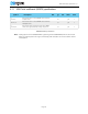
8.12 Analog to Digital Converter (ADC) specifications
Note: HFCLK XOSC is required to get the stated ADC accuracy.
Table 51 Analog to Digital Converter (ADC) specifications
Symbol Description Note Min. Typ. Max. Units
Tes t
level
DNL
10b
Differential non-linearity
(10 bit mode).
< 1 LSB 2
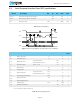
INL
10b
Integral non-linearity
(10 bit mode).
2 LSB 2
V
OS
Offset error. -2 +2 % 2
e
G
Gain error.
1
1. Source impedance less than 5 k.
-2 +2 % 2
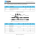
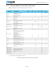
V
REF_VBG
Internal Band Gap reference
voltage (VBG).
1.20 V V 2
V
REF_VBG_ERR
Internal Band Gap reference
voltage error.
-1.5 +1.5 % 2
TC
REF_VBG_DRIFT
Internal Band Gap reference
voltage drift.
-200 +200 ppm/°C 2
V
REF_EXT
External reference voltage
(AREF0/1).
0.83 1.2 1.3 V 1
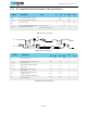
V
REF_VDD_LIM
Limited supply voltage range for
ADC using VDD with prescaler as
the reference.
CONFIG.REFSEL =
SupplyOneHalfPrescaling
CONFIG.REFSEL =
SupplyOneThirdPrescaling
1.7
2.5
2.6
3.6
V
V
1
1
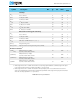
t
ADC10b
Time required to convert a single
sample in 10 bit mode.
68 µs 1
t
ADC9b
Time required to convert a single
sample in 9 bit mode.
36 µs 1
t
ADC8b
Time required to convert a single
sample in 8 bit mode.
20 µs 1
I
ADC
Current drawn by ADC during
conversion.
260 µA 1
ADC_ERR_1V8
Absolute error when used for
battery measurement at
1.8 V, 2.2 V, 2.6 V, 3.0 V, and
3.4 V.
2
2. Internal reference, input from VDD/3, 10 bit mode.
3 LSB 2
ADC_ERR_2V2 2 LSB 2
ADC_ERR_2V6 1 LSB 2
ADC_ERR_3V0 1 LSB 2
ADC_ERR_3V4 1 LSB 2