
Data Sheet

Page 56
nRF51822 Product Specification v3.1
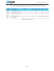
8.8 Serial Peripheral Interface Slave (SPIS) specifications
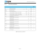
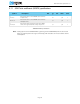
Table 44 SPIS specifications
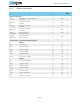
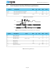
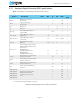
Figure 12 SPIS timing diagram, one byte transmission, SPI Mode 0
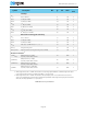
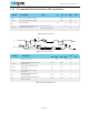
Table 45 SPIS timing parameters
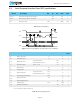
Symbol Description Min. Typ. Max. Units
Test
level
I
SPIS125K
Run current for SPI slave at 125 kbps.
1
1. CSN asserted.
180 µA 1
I
SPIS2M
Run current for SPI slave at 2 Mbps.
1
183 µA 1
f
SPIS
Bit rates for SPIS. 0.125 2 Mbps N/A
Symbol Description Note Min. Typ. Max. Units
Test
level
t
DC
Data to SCK setup. 10 ns 1
t
DH
SCK to Data hold. 10 ns 1
t
CSD
CSN to Data valid.
Low power mode.
1
Constant latency mode.
1
1. For more information on how to control the sub power modes, see the nRF51 Series Reference Manual.
7100
2100
ns 1
t
CD
SCK to Data Valid.
C
LOAD
= 10 pF
97
2
2. Increases/decreases with 1.2 ns/pF load.
ns 1
t
CL
SCK Low time. 40 ns 1
t
CH
SCK High time. 40 ns 1
t
CC
CSN to SCK Setup.
Low power mode.
1
Constant latency mode.
1
7000
2000
ns 1
t
CCH
Last SCK edge to CSN Hold. 2000 ns 1
t
CWH
CSN Inactive time. 300 ns 1
t
CDZ
CSN to Output High Z. 40 ns 1
f
SCK
SCK frequency. 0.125 2 MHz 1
t
R,
t
F
SCK Rise and Fall time. 100 ns 1
b
7
b
6
b
0
b
7
b
0
t
CD
t
DH
t
DC
t
CL
t
CH
SCK
MOSI
MISO
CSN
t
CWH
t
CDZ
t
CCH
t
CSD
t
CC