
Data Sheet

Page 30
nRF51822 Product Specification v3.1
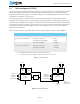
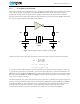
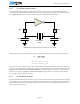
3.6.4 Synthesized 32.768 kHz clock
The low frequency clock can be synthesized from the high frequency clock. This saves the cost of a crystal
but increases average power consumption as the high frequency clock source will have to be active.
3.7 GPIO
The general purpose I/O is organized as one port with up to 32 I/Os (dependent on package) enabling
access and control of up to 32 pins through one port. Each GPIO can be accessed individually with the
following user configurable features:
•Input/output direction
• Output drive strength
• Internal pull-up and pull-down resistors
• Wake-up from high or low level triggers on all pins
• Trigger interrupt on all pins
• All pins can be used by the PPI task/event system; the maximum number of pins that can be
interfaced through the PPI at the same time is limited by the number of GPIOTE channels
• All pins can be individually configured to carry serial interface or quadrature demodulator
signals
3.8 Debugger support
The two pin Serial Wire Debug (SWD) interface provided as a part of the Debug Access Port (DAP) offers a
flexible and powerful mechanism for non-intrusive debugging of program code. Breakpoints and single
stepping are part of this support.