
Data Sheet

Page 17
nRF51822 Product Specification v3.1
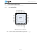
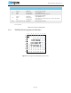
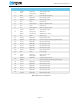
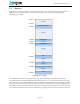
2.2.3.1 Ball functions CEAA and CFAC
Ball Name Function Description
A1
AVDD
Power Analog power supply (Radio).
A2
XC1
Analog input
Crystal connection for 16/32 MHz crystal oscillator or
external 16/32 MHz crystal reference.
A3
XC2
Analog output Crystal connection for 16/32 MHz crystal.
A4
DEC1
Power Power supply decoupling.
A5
P0.21
Digital I/O General purpose I/O.
A6
P0.24
Digital I/O General purpose I/O.
A7
P0.26
AIN0
XL2
Digital I/O
Analog input
Analog output
General purpose I/O.
ADC input 0.
Crystal connection for 32.768 kHz crystal oscillator.
A8
P0.27
AIN1
XL1
Digital I/O
Analog input
Analog input
General purpose I/O.
ADC input 1.
Crystal connection for 32.768 kHz crystal oscillator or
external 32.768 kHz crystal reference.
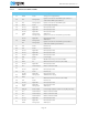
B1
VSS
Power Ground (0 V).
B4
VSS
Power Ground (0 V).
B5
P0.22
Digital I/O General purpose I/O.
B6
P0.23
Digital I/O General purpose I/O.
B7
P0.28
Digital I/O General purpose I/O.
B8
VDD
Power Power supply.
B9
DCC
Power DC/DC output voltage to external LC filter.
C1
ANT2
RF Differential antenna connection (TX and RX).
C5
P0.25
Digital I/O General purpose I/O.
C6
N.C.
No Connection Must be soldered to PCB.
C7
P0.29
Digital I/O General purpose I/O.
C8
VSS
Power Ground (0 V).
C9
P0.00
AREF0
Digital I/O
Analog input
General purpose I/O.
ADC Reference voltage.
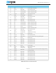
D1
ANT1
RF Differential antenna connection (TX and RX).
D7
VSS
Power Ground (0 V).
D8
P0.30
Digital I/O General purpose I/O.
D9
P0.02
AIN3
Digital I/O
Analog input
General purpose I/O.
ADC input 3.
E1
VDD_PA
Power output Power supply output (+1.6 V) for on-chip RF power amp.
E2
N.C.
No Connection Must be soldered to PCB.
E3
N.C.
No Connection Must be soldered to PCB.
E7
N.C.
No Connection Must be soldered to PCB.
E8
P0.31
Digital I/O General purpose I/O.
E9
P0.01
AIN2
Digital I/O
Analog input
General purpose I/O.
ADC input 2.