
Data Sheet

Page 13
nRF51822 Product Specification v3.1
Table 1 Pin functions QFN48 packet
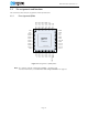
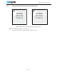
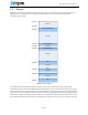
2.2.2 CDAB WLCSP ball assignment and functions
Figure 3 Ball assignment CDAB packet (top side view)
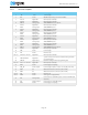
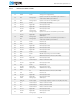
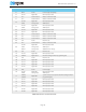
40 to 44
P0.21toP0.25 Digital I/O General purpose I/O pin.
45
P0.26
AIN0
XL2
Digital I/O
Analog input
Analog output
General purpose I/O pin.
ADC/LPCOMP input 0.
Connection for 32.768 kHz crystal.
46
P0.27
AIN1
XL1
Digital I/O
Analog input
Analog input
General purpose I/O pin.
ADC/LPCOMP input 1.
Connection for 32.768 kHz crystal or external 32.768 kHz
clock reference.
47, 48
P0.28andP0.29 Digital I/O General purpose I/O pin.
1. The exposed center pad of the QFN48 package must be connected to ground for proper
device operation.
Pin Pin name Pin function Description
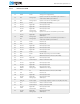
654321987
A
B
C
D
E
F
G
H
N51822
CDABHP
YYWWLL