nRF51822 Multiprotocol Bluetooth® low energy/2.4 GHz RF System on Chip Product Specification v3.1 Key Features • 2.4 GHz transceiver • -93 dBm sensitivity in Bluetooth® low energy mode • 250 kbps, 1 Mbps, 2 Mbps supported data rates • TX Power -20 to +4 dBm in 4 dB steps • TX Power -30 dBm Whisper mode • 13 mA peak RX, 10.5 mA peak TX (0 dBm) • 9.
nRF51822 Product Specification v3.1 Liability disclaimer Nordic Semiconductor ASA reserves the right to make changes without further notice to the product to improve reliability, function or design. Nordic Semiconductor ASA does not assume any liability arising out of the application or use of any product or circuits described herein.
nRF51822 Product Specification v3.1 Datasheet Status Status Description Objective Product Specification (OPS) This product specification contains target specifications for product development. Preliminary Product Specification (PPS) This product specification contains preliminary data; supplementary data may be published from Nordic Semiconductor ASA later. Product Specification (PS) This product specification contains final product specifications.
nRF51822 Product Specification v3.1 Date August 2014 Version Description 3.0 Update to reflect the changes in build code: • nRF51822-QFAA Hx0 • nRF51822-CEAA Ex0 • nRF51822-QFAB Cx0 (The x in the build codes can be any number between 0 and 9.) If you are working with a previous revision of the chip, read version 2.x of the document. Added content: • Section 8.5.3 “Radio current consumption with DC/DC enabled” on page 50 • Section 11.1.
nRF51822 Product Specification v3.1 Date October 2013 Version Description 2.0 This version of the document will target the nRF51822 QFAA G0 revision of the chip. If you are working with a previous revision of the chip, read version 1.3 or earlier of the document. Updated the following sections: Key Feature list on the front page, Chapter 1 “Introduction” on page 9, Section 2.1 “Block diagram” on page 10, Section 2.2 “Pin assignments and functions” on page 11, Section 3.2 “Memory” on page 20, Section 3.
nRF51822 Product Specification v3.1 Date Version Description April 2013 1.2 Added chip variant nRF51822-CEAA. Updated feature list on front page. Updated Section 3.2.1 on page 15, Section 3.2.2 on page 15, Chapter 6 on page 28, Section 10.4 on page 52, and Section 10.5.1 on page 53. Added Section 2.2.2 on page 10, Section 7.1 on page 29, Section 9.2 on page 50, and Section 11.3 on page 61. Removed PCB layouts in Chapter 11 on page 54. March 2013 1.1 Added chip variant nRF51822-QFAB.
nRF51822 Product Specification v3.1 Table of contents 1 1.1 1.2 Introduction............................................................................................................................................... 9 Required reading.............................................................................................................................................. 9 Writing conventions............................................................................................................
nRF51822 Product Specification v3.1 8.9 8.10 8.11 8.12 8.13 8.14 8.15 8.16 8.17 8.18 8.19 8.20 8.21 8.22 8.23 8.24 9 9.1 9.2 9.3 9.4 Serial Peripheral Interface (SPI) Master specifications ......................................................................57 I2C compatible Two Wire Interface (TWI) specifications..................................................................58 GPIO Tasks and Events (GPIOTE) specifications................................................................................
nRF51822 Product Specification v3.1 1 Introduction The nRF51822 is an ultra-low power 2.4 GHz wireless System on Chip (SoC) integrating the nRF51 series 2.4 GHz transceiver, a 32 bit ARM® Cortex™-M0 CPU, flash memory, and analog and digital peripherals. nRF51822 can support Bluetooth® low energy and a range of proprietary 2.4 GHz protocols, such as Gazell from Nordic Semiconductor. Fully qualified Bluetooth low energy stacks for nRF51822 are implemented in the S100 series of SoftDevices.
nRF51822 Product Specification v3.1 2 Product overview 2.1 Block diagram 5$0 5$0 5$0 VODYH VODYH VODYH 6:&/. 5$0 VODYH Q5) QP *3,2 VODYH 6: '3 6:',2 3 3 ± 3 VODYH VODYH &38 VODYH '$3 VODYH PDVWHU $+% 0XOWL /D\HU $+% 72 $3% %5,'*( ),&5 8,&5 &2'( $50 &257(; 0 19,& Q5(6(7 190& 51* 32:(5 57& > Q@ 7,0(5 > Q@ :'7 7(03 33, (&% ;& ;& ;/ &/2&.
nRF51822 Product Specification v3.1 2.2 Pin assignments and functions This section describes the pin assignment and the pin functions. 37 38 39 40 41 42 43 44 45 46 1 36 2 35 3 34 4 33 5 32 N51822 nRF5102 QFVVHP QFN48 YYWWLL 6 7 8 31 30 29 9 28 10 27 exposed die pad AVDD AVDD VSS VSS ANT2 ANT1 VDD_PA DEC2 P0.20 P0.19 P0.18 P0.17 24 23 22 21 20 19 18 17 16 25 15 26 12 14 11 13 VDD DCC P0.30 P0.00 P0.01 P0.02 P0.03 P0.04 P0.05 P0.06 P0.07 VDD 47 48 P0.29 P0.
nRF51822 Product Specification v3.1 2.2.1.1 Pin functions QFN48 Pin Pin name Pin function Description 1 VDD Power Power supply. 2 DCC Power DC/DC output voltage to external LC filter. 3 P0.30 Digital I/O General purpose I/O pin. 4 P0.00 AREF0 Digital I/O Analog input General purpose I/O pin. ADC/LPCOMP reference input 0. 5 P0.01 AIN2 Digital I/O Analog input General purpose I/O pin. ADC/LPCOMP input 2. 6 P0.02 AIN3 Digital I/O Analog input General purpose I/O pin.
nRF51822 Product Specification v3.1 Pin 40 to 44 Pin name Pin function Description P0.21 to P0.25 Digital I/O General purpose I/O pin. 45 P0.26 AIN0 XL2 Digital I/O Analog input Analog output General purpose I/O pin. ADC/LPCOMP input 0. Connection for 32.768 kHz crystal. 46 P0.27 AIN1 XL1 Digital I/O Analog input Analog input General purpose I/O pin. ADC/LPCOMP input 1. Connection for 32.768 kHz crystal or external 32.768 kHz clock reference. P0.28 and P0.
nRF51822 Product Specification v3.1 2.2.2.1 Ball functions CDAB Ball Name Function Description A1 AVDD Power Analog power supply (Radio). A2 XC1 Analog input Crystal connection for 16/32 MHz crystal oscillator or external 16/32 MHz crystal reference. A3 XC2 Analog output Crystal connection for 16/32 MHz crystal. A4 DEC1 Power Power supply decoupling. A5 P0.21 Digital I/O General purpose I/O. A6 P0.24 Digital I/O General purpose I/O. A7 P0.
nRF51822 Product Specification v3.1 Ball Name Function Description E9 P0.03 AIN4 Digital I/O Analog input General purpose I/O. ADC input 4. F1 DEC2 Power Power supply decoupling. F2 P0.19 Digital I/O General purpose I/O. F3 P0.18 Digital I/O General purpose I/O. F4 VSS Power Ground (0 V). F5 N.C. No Connection Must be soldered to PCB. F6 VSS Power Ground (0 V). F7 N.C. No Connection Must be soldered to PCB. F8 P0.
nRF51822 Product Specification v3.1 2.2.3 CEAA and CFAC WLCSP ball assignment and functions 1 2 3 4 5 6 7 8 9 1 A A B B C D E F C N51822 CEAAHP YYWWLL D E F G G H H J J 2 3 4 5 6 N51822 CFACHP YYWWLL Figure 4 Ball assignment CEAA and CFAC packet (top side view) Note: HP = Buildcode, YYWWLL = Tracking code Solder balls not visible on the top side. Dot denotes A1 corner.
nRF51822 Product Specification v3.1 2.2.3.1 Ball functions CEAA and CFAC Ball Name Function Description A1 AVDD Power Analog power supply (Radio). A2 XC1 Analog input Crystal connection for 16/32 MHz crystal oscillator or external 16/32 MHz crystal reference. A3 XC2 Analog output Crystal connection for 16/32 MHz crystal. A4 DEC1 Power Power supply decoupling. A5 P0.21 Digital I/O General purpose I/O. A6 P0.24 Digital I/O General purpose I/O. A7 P0.
nRF51822 Product Specification v3.1 Ball Name Function Description F1 DEC2 Power Power supply decoupling. F2 P0.19 Digital I/O General purpose I/O. F3 N.C. No Connection Must be soldered to PCB. F7 N.C. No Connection Must be soldered to PCB. F8 P0.04 AIN5 Digital I/O Analog input General purpose I/O. ADC input 5. F9 P0.03 AIN4 Digital I/O Analog input General purpose I/O. ADC input 4. G1 P0.20 Digital I/O General purpose I/O. G2 P0.17 Digital I/O General purpose I/O.
nRF51822 Product Specification v3.1 3 System blocks The chip contains system-level features common to all nRF51 series devices including clock control, power and reset, interrupt system, Programmable Peripheral Interconnect (PPI), watchdog, and GPIO. System blocks which have a register interface and/or interrupt vector assigned are instantiated in the device address space.
nRF51822 Product Specification v3.1 3.2 Memory All memory and registers are found in the same address space as shown in the Device Memory Map, see Figure 5. Devices in the nRF51 series use flash based memory in the code, FICR, and UICR regions. The RAM region is SRAM.
nRF51822 Product Specification v3.1 3.2.1 Code organization Chip variant Code size Page size No of pages nRF51822-QFAA nRF51822-CEAA 256 kB 1024 byte 256 nRF51822-QFAB nRF51822-CDAB 128 kB 1024 byte 128 nRF51822-QFAC nRF51822-CFAC 256 kB 1024 byte 256 Table 4 Code organization 3.2.2 RAM organization RAM is divided into blocks for separate power management which is controlled by the POWER System Block. Each block is divided into two 4 kByte RAM sections with separate RAM AHB slaves.
nRF51822 Product Specification v3.1 Table 6 and Table 7 shows how memory allocated to different functions can be distributed between RAM sections for parallel access. There is a table for chip variants with 16 kB or 32 kB RAM.
nRF51822 Product Specification v3.1 3.4 3.4.1 Power management (POWER) Power supply nRF51 supports three different power supply alternatives: • Internal LDO setup • DC/DC converter setup • Low voltage mode setup See Table 20 on page 38 for the voltage range on the different alternatives. See Chapter 11 “Reference circuitry” on page 76 for details on the schematic used for the different power supply alternatives. 3.4.1.
nRF51822 Product Specification v3.1 3.4.2 Power management The power management system is highly flexible with functional blocks such as the CPU, Radio Transceiver, and peripherals having separate power state control in addition to the global System ON and OFF modes. In System OFF mode, RAM can be retained and the device state can be changed to System ON through Reset, GPIO DETECT signal, or LPCOMP ANADETECT signal.
nRF51822 Product Specification v3.1 3.4.2.2 System ON mode In system ON mode the system is fully operational and the CPU and selected peripherals can be brought into a state where they are functional and more or less responsive depending on the sub-power mode selected. There are two sub-power modes: • Low power • Constant latency Low Power In Low Power mode the automatic power management system is optimized to save power. This is done by keeping as much as possible of the system powered down.
nRF51822 Product Specification v3.1 3.5 Programmable Peripheral Interconnect (PPI) The Programmable Peripheral Interconnect (PPI) enables peripherals to interact autonomously with each other using tasks and events independent of the CPU. The PPI allows precise synchronization between peripherals when real-time application constraints exist and eliminates the need for CPU activity to implement behavior which can be predefined using PPI.
nRF51822 Product Specification v3.1 3.6 Clock management (CLOCK) The advanced clock management system can source the system clocks from a range of internal or external high and low frequency oscillators and distribute them to modules based upon a module’s individual requirements. This prevents large clock trees from being active and drawing power when system modules needing this clock reference are not active.
nRF51822 Product Specification v3.1 3.6.1 16/32 MHz crystal oscillator The crystal oscillator can be controlled either by a 16 MHz or a 32 MHz external crystal. However, the system clock is always 16 MHz, see the nRF51 Series Reference Manual for more details. The crystal oscillator is designed for use with an AT-cut quartz crystal in parallel resonant mode. To achieve correct oscillation frequency, the load capacitance must match the specification in the crystal data sheet.
nRF51822 Product Specification v3.1 3.6.2 32.768 kHz crystal oscillator The 32.768 kHz crystal oscillator is designed for use with a quartz crystal in parallel resonant mode. To achieve correct oscillation frequency, the load capacitance must match the specification in the crystal data sheet. Figure 8 shows how the crystal is connected to the 32.768 kHz crystal oscillator. XL1 XL2 C1 C2 32.768 kHz crystal Figure 8 Circuit diagram of the 32.
nRF51822 Product Specification v3.1 3.6.4 Synthesized 32.768 kHz clock The low frequency clock can be synthesized from the high frequency clock. This saves the cost of a crystal but increases average power consumption as the high frequency clock source will have to be active. 3.7 GPIO The general purpose I/O is organized as one port with up to 32 I/Os (dependent on package) enabling access and control of up to 32 pins through one port.
nRF51822 Product Specification v3.1 4 Peripheral blocks Peripheral blocks which have a register interface and/or interrupt vector assigned are instantiated, one or more times, in the device address space. The instances, associated ID (for those with interrupt vectors), and base address of features are found in Table 18 on page 36. Detailed functional descriptions, configuration options, and register interfaces can be found in the nRF51 Series Reference Manual. 4.1 2.
nRF51822 Product Specification v3.1 4.2 Timer/counters (TIMER) The timer/counter runs on the high-frequency clock source (HFCLK) and includes a 4 bit (1/2X) prescaler that can divide the HFCLK. The TIMER will start requesting the 1 MHz mode of the HFCLK for values of the prescaler that gives fTIMER less or equal to 1 MHz. If the timer module is the only one requesting the HFCLK, the system will automatically switch to using the 1 MHz mode resulting in a decrease in the current consumption.
nRF51822 Product Specification v3.1 4.5 AES CCM Mode Encryption (CCM) Cipher Block Chaining - Message Authentication Code (CCM) Mode is an authenticated encryption algorithm designed to provide both authentication and confidentiality during data transfer. CCM combines counter mode encryption and CBC-MAC authentication.
nRF51822 Product Specification v3.1 4.9 Temperature sensor (TEMP) The temperature sensor measures die temperature over the temperature range of the device with 0.25° C resolution. 4.10 Serial Peripheral Interface (SPI/SPIS) The SPI interfaces enable full duplex synchronous communication between devices. They support a threewire (SCK, MISO, MOSI) bi-directional bus with fast data transfers.
nRF51822 Product Specification v3.1 4.12 Universal Asynchronous Receiver/Transmitter (UART) The Universal Asynchronous Receiver/Transmitter offers fast, full-duplex, asynchronous serial communication with built-in flow control (CTS, RTS) support in hardware up to 1 Mbps baud. Parity checking is supported. The GPIOs used for each UART interface line can be chosen from any GPIO on the device and are independently configurable.
nRF51822 Product Specification v3.1 5 Instance table The peripheral instantiation of the chip is shown in the table below. ID Base address Peripheral Instance Description 0 0x40000000 POWER POWER Power Control. 0 0x40000000 CLOCK CLOCK Clock Control. 0 0x40000000 MPU MPU Memory Protection Unit. 1 0x40001000 RADIO RADIO 2.4 GHz Radio. 2 0x40002000 UART UART0 Universal Asynchronous Receiver/Transmitter. 3 0x40003000 SPI SPI0 SPI Master.
nRF51822 Product Specification v3.1 6 Absolute maximum ratings Maximum ratings are the extreme limits the chip can be exposed to without causing permanent damage. Exposure to absolute maximum ratings for prolonged periods of time may affect the reliability of the chip. Table 19 specifies the absolute maximum ratings. Symbol Parameter Min. Max. Unit -0.3 +3.9 V DEC2 2 V VSS 0 V -0.3 VDD + 0.
nRF51822 Product Specification v3.1 7 Operating conditions The operating conditions are the physical parameters that the chip can operate within as defined in Table 20. Symbol Parameter Notes Min. Typ. Max. Units VDD Supply voltage, internal LDO setup 1.8 3.0 3.6 V VDD Supply voltage, DC/DC converter setup 2.1 3.0 3.6 V VDD Supply voltage, low voltage mode setup 1 1.75 1.8 1.95 V tR_VDD Supply rise time (0 V to VDD) 2 100 ms TA Operating temperature 75 °C -25 25 1.
nRF51822 Product Specification v3.1 8 Electrical specifications This chapter contains electrical specifications for device interfaces and peripherals including radio parameters and current consumption. The test levels referenced are defined in Table 21. Test level Description 1 Simulated, calculated, by design (specification limit) or prototype samples tested at NOC. 2 Parameters have been verified at Test level 1 and in addition: Prototype samples tested at EOC.
nRF51822 Product Specification v3.1 8.1.2 16 MHz crystal oscillator (16M XOSC) Symbol Description Note Min. Typ. Max. Units Test level MHz N/A fNOM,X16M Crystal frequency. fTOL,X16M Frequency tolerance.1 ±502 ppm N/A fTOL,X16M,BLE Frequency tolerance, Bluetooth low energy applications.1 ±402 ppm N/A RS,X16M Equivalent series resistance. 100 150 200 Ω Ω Ω N/A N/A N/A PD,X16M Drive level. 100 μW N/A Cpin Input capacitance on XC1 and XC2 pads.
nRF51822 Product Specification v3.1 8.1.3 32 MHz crystal oscillator (32M XOSC) Symbol Description Note Min. Typ. Max. Units Test level 32 MHz N/A fNOM,X32M Crystal frequency. fTOL,X32M Frequency tolerance.1 ±502 ppm N/A fTOL,X32M,BLE Frequency tolerance, Bluetooth low energy applications.1 ±402 ppm N/A RS,X32M Equivalent series resistance. 60 80 100 Ω Ω Ω N/A N/A N/A PD,X32M Drive level. 100 μW N/A Cpin Input capacitance on XC1 and XC2 pads.
nRF51822 Product Specification v3.1 8.1.4 16 MHz RC oscillator (16M RCOSC) Symbol Description Min. Typ. fNOM,RC16M Nominal frequency. 16 fTOL,RC16M Frequency tolerance. ±1 IRC16M Run current for 16 MHz RC oscillator. 7501 IRC16M,1M Run current for 16 MHz RCOSC when used only for a Timer at 1 MHz or less. 5401 tSTART,RC16M Startup time for 16 MHz RC oscillator. 4.2 IRC16M, START Startup current for 16 MHz RC oscillator. 400 Max. ±5 5.
nRF51822 Product Specification v3.1 8.1.6 Symbol 32.768 kHz RC oscillator (32k RCOSC) Description Note Min. Typ. Max. Units Test level fNOM,RC32k Nominal frequency. 32.768 kHz N/A fTOL,RC32k Frequency tolerance. ±2 % 3 fTOL,CAL,RC32k Frequency tolerance. ±250 ppm 1 IRC32k Run current. 0.8 1.1 μA 1 tSTART,RC32k Startup time. 390 487 μs 1 Calibration interval 4 s 0.5 Table 26 32.768 kHz RC oscillator 8.1.7 32.
nRF51822 Product Specification v3.1 8.2 Power management Symbol Description Note VPOF Nominal power level warning thresholds (falling supply voltage). VTOL Threshold voltage tolerance. VHYST Threshold voltage hysteresis. Min. Typ. Max. Units Test level V 2 % 3 mV 3 2.1 2.3 2.5 2.7 Accuracy as defined by VTOL ±5 VPOF = 2.1 V VPOF = 2.3 V VPOF = 2.5 V VPOF = 2.7 V 46 62 79 100 Table 28 Power Fail Comparator Symbol Description Min. Typ. Max.
nRF51822 Product Specification v3.1 Power on reset time (tPOR) is the time from when the supply starts rising to when the device comes out of reset and the CPU starts. The time increases with, and is inclusive of, supply rise time from 0 V to VDD. Table 30 gives tPOR for a number of supply rise times, simulated with a linear ramp from 0 V to VDD, over the supply voltage range 1.8 V to 3.6 V. Symbol Description Note Min. Typ. Max.
nRF51822 Product Specification v3.1 Symbol Description Note Min. Typ. Max. Units Test level IOFF Current in SYSTEM OFF, no RAM retention. 0.61 μA 2 IOFF, RET, 8k Additional current in SYSTEM OFF per retained RAM block (8 kB) 0.61 μA 2 IOFF2ON OFF to CPU execute transition current. 400 μA 1 tOFF2ON OFF to CPU execute. 9.6 μs 1 ION,16k SYSTEM-ON base current with 16 kB RAM enabled. 2.61 μA 2 ION,32k SYSTEM-ON base current with 32 kB RAM enabled. 3.
nRF51822 Product Specification v3.1 Symbol Description Note t1V7 Startup time for 1V7 regulator I1V7 Current drawn by 1V7 regulator FDCDC DC/DC converter current conversion factor. 1. 2. 3. 4. Min. Typ. Max. 2 3.6 105 0.654 Units Test level μs 1 μA 2 1.24 Add 1 μA to the current value if the device is used in Low voltage mode. This number includes the current used by the automated power and clock management system. For details on 1 MHz mode, see Section 4.
nRF51822 Product Specification v3.1 8.3 Block resource requirements Resource requirements Block ID 1V2 HFCLK1 Comment LFCLK 1V7 Radio 1 x x Requires HFCLK XOSC. UART 2 x x When receiver or transmitter are STARTed. SPIS 4 x x Requested when CSN asserts. SPI 3, 4 x x TWI 3, 4 x x GPIOTE 6 x x Only in input mode. ADC 7 x x Requires HFCLK XOSC. x Requires 1V2 when a TIMER EVENT is triggered.
nRF51822 Product Specification v3.1 8.5 Radio transceiver 8.5.1 General radio characteristics Symbol Description Note Min. 1 MHz channel spacing. Max. Units Test level 2483 MHz N/A 1 MHz N/A Typ. fOP Operating frequencies. PLLres PLL programming resolution. Δf250 Frequency deviation at 250 kbps. ±170 kHz 2 Δf1M Frequency deviation at 1 Mbps. ±170 kHz 2 Δf2M Frequency deviation at 2 Mbps. ±320 kHz 2 ΔfBLE Frequency deviation at BLE.
nRF51822 Product Specification v3.1 8.5.3 Radio current consumption with DC/DC enabled Symbol Description Note Min. Typ. Max. Units Test level ITX,+4dBm TX only run current at POUT = +4 dBm. 1 11.8 mA 2 ITX,0dBm TX only run current at POUT = 0 dBm. 1 8.0 mA 2 ITX,-4dBm TX only run current at POUT = -4 dBm. 1 6.3 mA 2 ITX,-8dBm TX only run current at POUT = -8 dBm. 1 5.6 mA 2 ITX,-12dBm TX only run current at POUT = -12 dBm. 1 5.
nRF51822 Product Specification v3.1 8.5.4 Transmitter specifications Symbol Description Min. Units Test level 4 dBm 4 24 dB 2 dB 1 dBm 2 Typ. Max. PRF Maximum output power. PRFC RF power control range. PRFCR RF power accuracy. PWHISP RF power whisper mode. PBW2 20 dB bandwidth for modulated carrier (2 Mbps). 1800 2000 kHz 2 PBW1 20 dB bandwidth for modulated carrier (1 Mbps). 950 1100 kHz 2 PBW250 20 dB bandwidth for modulated carrier (250 kbps).
nRF51822 Product Specification v3.1 8.5.5 Symbol Receiver specifications Description Min. Units Test level 0 dBm 1 Typ. Max. Receiver operation PRXMAX Maximum received signal strength at < 0.1% PER. PRXSENS,2M Sensitivity (0.1% BER) at 2 Mbps. -85 dBm 2 PRXSENS,1M Sensitivity (0.1% BER) at 1 Mbps. -90 dBm 2 PRXSENS,250k Sensitivity (0.1% BER) at 250 kbps. -96 dBm 2 PSENS IT 1 Mbps BLE Receiver sensitivity: Ideal transmitter.
nRF51822 Product Specification v3.1 Symbol Description Min. Units Test level 4 dB 2 Typ. Max. 250 kbps C/ICO C/I co-channel. C/I1ST 1st ACS, C/I 1 MHz. -10 dB 2 C/I2ND 2nd ACS, C/I 2 MHz. -34 dB 2 C/I3RD 3rd ACS, C/I 3 MHz. -39 dB 2 th C/I6th 6 ACS, C/I fi > 6 MHz. -50 dB 2 C/I12th 12th ACS, C/I 12 MHz. -55 dB 2 C/INth Nth ACS, C/I fi > 25 MHz. -60 dB 2 Bluetooth Low Energy RX selectivity C/ICO C/I co-channel. 10 dB 2 C/I1ST 1st ACS, C/I 1 MHz.
nRF51822 Product Specification v3.1 8.5.6 Radio timing parameters Symbol Description 250 k 1M 2M BLE Jitter Units tTXEN Time between TXEN task and READY event. 132 132 132 140 0 μs tTXDISABLE Time between DISABLE task and DISABLED event when the radio was in TX. 10 4 3 4 1 μs tRXEN Time between the RXEN task and READY event. 130 130 130 138 0 μs tRXDISABLE Time between DISABLE task and DISABLED event when the radio was in RX. 0 0 0 0 1 μs tTXCHAIN TX chain delay.
nRF51822 Product Specification v3.1 8.7 Universal Asynchronous Receiver/Transmitter (UART) specifications Symbol Description Note Min. Typ. Max. Units Test level IUART1M Run current at max baud rate. 230 μA 1 IUART115k Run current at 115200 bps. 220 μA 1 IUART1k2 Run current at 1200 bps. 210 μA 1 fUART Baud rate for UART. kbps N/A tCTSH CTS high time. μs 1 1.
nRF51822 Product Specification v3.1 8.8 Serial Peripheral Interface Slave (SPIS) specifications Symbol Description Min. Typ. Max. Units Test level ISPIS125K Run current for SPI slave at 125 kbps.1 180 μA 1 ISPIS2M Run current for SPI slave at 2 Mbps.1 183 μA 1 fSPIS Bit rates for SPIS. Mbps N/A Units Test level 0.125 2 1. CSN asserted.
nRF51822 Product Specification v3.1 8.9 Serial Peripheral Interface (SPI) Master specifications Symbol Description Min. Typ. Max. Units Test level ISPI125K Run current for SPI master at 125 kbps. 180 μA 1 ISPI4M Run current for SPI master at 4 Mbps. 200 μA 1 fSPI Bit rates for SPI. Mbps N/A Units Test level 0.
nRF51822 Product Specification v3.1 8.10 I2C compatible Two Wire Interface (TWI) specifications Symbol Description Note Min. Typ. Max. Units Test level I2W100K Run current for TWI at 100 kbps. 380 μA 1 I2W400K Run current for TWI at 400 kbps. 400 μA 1 f2W Bit rates for TWI. kbps N/A tTWI,START Time from STARTRX/STARTTX task is given until start condition. μs 1 100 Low power mode.1 Constant latency mode.1 400 3 1 4.4 1.
nRF51822 Product Specification v3.1 8.11 GPIO Tasks and Events (GPIOTE) specifications Symbol Description Min. Typ. Max. Units Test level IGPIOTE,IN Run current with 1 or more GPIOTE active channels in Input mode. 22 μA 1 IGPIOTE,OUT Run current with 1 or more GPIOTE active channels in Output mode. 0.1 μA 1 IGPIOTE,IDLE Run current when all channels in Idle mode. PORT event can be generated with a delay of up to t1V2. 0.
nRF51822 Product Specification v3.1 8.12 Analog to Digital Converter (ADC) specifications Note: HFCLK XOSC is required to get the stated ADC accuracy. Symbol Description Note Min. DNL10b Differential non-linearity (10 bit mode). INL10b Integral non-linearity (10 bit mode). VOS Offset error. eG Gain error. VREF_VBG Internal Band Gap reference voltage (VBG). VREF_VBG_ERR Internal Band Gap reference voltage error. -1.5 TCREF_VBG_DRIFT Internal Band Gap reference voltage drift.
nRF51822 Product Specification v3.1 8.13 Timer (TIMER) specifications Symbol Description Note Min. Typ. Max. Units Test level ITIMER0/1/2 Timer current when running from HFCLK in 16 MHz mode. 30 μA 1 ITIMER0/1/2,1M Timer current when running from HFCLK in 1 MHz mode. 4 μA 1 tTIMER,START Time from START task is given until timer starts counting. 0.25 μs 1 Units Test level μA 1 Units Test level Table 52 Timer specifications 8.
nRF51822 Product Specification v3.1 8.16 Random Number Generator (RNG) specifications Symbol Description Note Min. Units Test level 60 μA 1 Typ. Max. IRNG Run current at 16 MHz. tRNG,RAW Run time per byte in RAW mode. Uniform distribution of 0 and 1 is not guaranteed. 167 μs 1 Run time per byte in Uniform mode. Uniform distribution of 0 and 1 is guaranteed. Time to generate a byte cannot be guaranteed. 677 μs 1 tRNG,UNI Table 55 Random Number Generator (RNG) specifications 8.
nRF51822 Product Specification v3.1 8.20 Watchdog Timer (WDT) specifications Symbol Description Min. IWDT Run current for watchdog timer. tWDT Time out interval, watchdog timer. Typ. Max. 0.1 30 μs Units Test level μA 1 36 hrs 1 Table 59 Watchdog Timer specifications 8.21 Quadrature Decoder (QDEC) specifications Symbol Description Note Min. IQDEC Typ. Max. 12 tSAMPLE Time between sampling signals from quadrature decoder.
nRF51822 Product Specification v3.1 8.22 Non-Volatile Memory Controller (NVMC) specifications Flash write is done by executing a program that writes one word (32 bit) consecutively after the other to the flash memory. The program doing the flash writes could be set up to run from flash or from RAM. The timing of one flash write operation depends on whether the next instructions following the flash write will be fetched from flash or from RAM.
nRF51822 Product Specification v3.1 8.23 General Purpose I/O (GPIO) specifications Symbol Parameter (condition) Note Min. Typ. Max. Units VIH Input high voltage. 0.7 VDD VDD V VIL Input low voltage. VSS 0.3 VDD V VOH Output high voltage (std. drive, 0.5 mA). VDD-0.3 VDD V VOH Output high voltage (high-drive, 5 mA). VDD-0.3 VDD V VOL Output low voltage (std. drive, 0.5 mA). VSS 0.3 V VOL Output low voltage (high-drive, 5 mA). VSS 0.3 V RPU Pull-up resistance.
nRF51822 Product Specification v3.1 9 Mechanical specifications This chapter covers the mechanical specifications for all chip variants of the nRF51822. The following table lists the cross references to the package sections describing each package variant. Package Cross references QFN48 Section 9.1 “QFN48 package” on page 66 CDAB Section 9.2 “CDAB WLCSP package” on page 67 CEAA Section 9.3 “CEAA WLCSP package” on page 68 CFAC Section 9.
nRF51822 Product Specification v3.1 9.2 CDAB WLCSP package Figure 16 CDAB WLCSP package Package CDAB WLCSP A A1 A3 b D E D2 E2 e K L 0.50 0.55 0.12 0.15 0.18 0.33 0.35 0.37 0.16 0.20 0.24 3.45 3.50 3.55 3.28 3.33 3.38 3.2 2.8 0.4 1.41 1.61 Table 66 CDAB WLCSP package dimensions in millimeters Page 67 Min. Nom. Max.
nRF51822 Product Specification v3.1 9.3 CEAA WLCSP package Figure 17 CEAA WLCSP package Package CEAA WLCSP A A1 A3 b D E D2 E2 e K L 0.50 0.55 0.12 0.15 0.18 0.33 0.35 0.37 0.16 0.20 0.24 3.45 3.50 3.55 3.78 3.83 3.88 3.2 3.2 0.4 1.66 1.61 Table 67 CEAA WLCSP package dimensions in millimeters Page 68 Min. Nom. Max.
nRF51822 Product Specification v3.1 9.4 CFAC WLCSP package Figure 18 CFAC WLCSP package Package CFAC WLCSP A A1 A3 b D E D2 E2 e K L 0.50 0.55 0.12 0.15 0.18 0.33 0.35 0.37 0.16 0.20 0.24 3.78 3.83 3.88 3.78 3.83 3.88 3.2 3.2 0.4 1.66 1.78 Table 68 CFAC WLCSP package dimensions in millimeters Page 69 Min. Nom. Max.
nRF51822 Product Specification v3.1 10 Ordering information 10.1 Chip marking N 5 1 8 2 2
Table 69 Package marking 10.
nRF51822 Product Specification v3.1 10.3 Outer box label FROM: TO: DEVICE: NRFxxxxx-- S/O No.: CUSTOMER PO No.: WF LOT No.: Trace Code: QTY: PACKAGE COUNT: PACKAGE WEIGHT: of KGS COUNTRY OF ORIGIN: Figure 20 Outer box label 10.
nRF51822 Product Specification v3.1 10.5 Abbreviations Abbreviation Definition and Implemented Codes N51/nRF51 nRF51 series product 822 Part code Package code Variant code Build code H - Hardware version code P - Production configuration code (production site, etc.
nRF51822 Product Specification v3.1 10.6 Code ranges and values Packet Size (mm) Pin/Ball Count Pitch (mm) QF QFN 6x6 48 0.4 CD WLCSP 3.50 x 3.33 56 0.4 CE WLCSP 3.50 x 3.83 62 0.4 CF WLCSP 3.83 x 3.83 62 0.4 Table 72 Package codes Flash (kB) RAM (kB) DC/DC Bond-out AA 256 16 YES AB 128 16 YES AC 256 32 YES Table 73 Variant codes [A. .
nRF51822 Product Specification v3.1 Description [1. .52] Week of production Table 78 Week codes [AA. .
nRF51822 Product Specification v3.1 10.7 10.7.1 Product options nRF ICs MOQ1 Order code nRF51822-QFAA-R7 nRF51822-QFAB-R7 nRF51822-QFAC-R7 1000 nRF51822-QFAA-R nRF51822-QFAB-R nRF51822-QFAC-R 3000 nRF51822-CEAA-R7 nRF51822-CDAB-R7 nRF51822-CFAC-R7 1500 nRF51822-CEAA-R nRF51822-CDAB-R nRF51822-CFAC-R 7000 nRF51822-QFAA-T nRF51822-QFAB-T nRF51822-QFAC-T 490 1. Minimum Order Quantity. Table 81 Order code 10.7.2 Development tools Order code Description nRF51-DK1 nRF51 Bluetooth Smart/ANT/2.
nRF51822 Product Specification v3.1 11 Reference circuitry For the following reference layouts, C_pcb1 and C_pcb2, between X1 and XC1/XC2, is estimated to 0.5 pF each. The exposed center pad of the QFN48 package must be connected to supply ground for proper device operation. 11.1 PCB guidelines A well designed PCB is necessary to achieve good RF performance. A poor layout can lead to loss in performance or functionality.
nRF51822 Product Specification v3.1 11.1.1 PCB layout example The PCB layout shown in Figure 21 is a reference layout for the QFN package with internal LDO setup. For all available reference layouts, see the Reference Layout section on the Downloads tab for the different chip variants on www.nordicsemi.com.
nRF51822 Product Specification v3.1 11.2 Reference design schematics The following sections covers the reference design schematics for all chip variants of the nRF51822. Table 83 lists the cross references to the package sections describing each package variant. For package See section: QFAA Section 11.3 “QFAA QFN48 package” on page 79 QFAB Section 11.4 “QFAB QFN48 package” on page 85 QFAC Section 11.5 “QFAC QFN48 package” on page 91 CDAB Section 11.
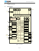
nRF51822 Product Specification v3.1 11.3 QFAA QFN48 package Documentation for the QFAA QFN48 package reference circuit, including Altium Designer files, PCB layout files, and PCB production files can be downloaded from www.nordicsemi.com. 11.3.1 QFAA QFN48 schematic with internal LDO setup Optional C13 C1 12pF C14 12pF X2 32.768kHz C2 12pF X1 16MHz 12pF P0.29 P0.28 XL1 XL2 P0.25 P0.24 P0.23 P0.22 P0.21 C8 100nF 48 47 46 45 44 43 42 41 40 39 38 37 VCC_nRF C7 100nF VCC_nRF C11 C9 1.
nRF51822 Product Specification v3.1 11.3.1.1 Bill of Materials Designator Value Description Footprint C1, C2, C13, C14 12 pF Capacitor, NP0, ±2% 0402 C3 2.2 nF Capacitor, X7R, ±10% 0402 C4 1.0 pF Capacitor, NP0, ±0.1 pF 0402 C5 2.2 pF Capacitor, NP0, ±0.1 pF 0402 C6 1.5 pF Capacitor, NP0, ±0.1 pF 0402 C7, C8, C11 100 nF Capacitor, X7R, ±10% 0402 C9 1.0 nF Capacitor, X7R, ±10% 0402 C10 47 nF Capacitor, X7R, ±10% 0402 L1 4.
nRF51822 Product Specification v3.1 11.3.2 QFAA QFN48 schematic with low voltage mode setup Optional C13 C1 12pF C14 12pF X2 32.768kHz C2 12pF X1 16MHz 12pF P0.29 P0.28 XL1 XL2 P0.25 P0.24 P0.23 P0.22 P0.21 C8 100nF 48 47 46 45 44 43 42 41 40 39 38 37 VCC_1V8 C7 100nF VCC_1V8 C11 P0.29 P0.28 P0.27 P0.26 P0.25 P0.24 P0.23 P0.22 P0.21 DEC1 XC2 XC1 1 2 3 4 5 6 7 8 9 10 11 12 VDD DCC P0.30 P0.00 P0.01 P0.02 P0.03 P0.04 P0.05 P0.06 P0.07 VDD AVDD AVDD VSS VSS ANT2 ANT1 VDD_PA DEC2 P0.20 P0.
nRF51822 Product Specification v3.1 11.3.2.1 Bill of Materials Designator Value Description Footprint C1, C2, C13, C14 12 pF Capacitor, NP0, ±2% 0402 C3 2.2 nF Capacitor, X7R, ±10% 0402 C4 1.0 pF Capacitor, NP0, ±0.1 pF 0402 C5 2.2 pF Capacitor, NP0, ±0.1 pF 0402 C6 1.5 pF Capacitor, NP0, ±0.1 pF 0402 C7, C8, C11 100 nF Capacitor, X7R, ±10% 0402 C9 1.0 nF Capacitor, X7R, ±10% 0402 C10 47 nF Capacitor, X7R, ±10% 0402 L1 4.
nRF51822 Product Specification v3.1 11.3.3 QFAA QFN48 schematic with DC/DC converter setup Optional C13 C1 12pF C14 12pF X2 32.768kHz C2 12pF X1 16MHz 12pF P0.29 P0.28 XL1 XL2 P0.25 P0.24 P0.23 P0.22 P0.21 C8 100nF 48 47 46 45 44 43 42 41 40 39 38 37 AVDD L5 L4 15nH 10μH C12 1.0μF P0.30 P0.00 C7 P0.01 4.7μF P0.02 P0.03 P0.04 P0.05 P0.06 VCC_nRF P0.07 C11 C9 1.0nF P0.29 P0.28 P0.27 P0.26 P0.25 P0.24 P0.23 P0.22 P0.21 DEC1 XC2 XC1 VDD DCC P0.30 P0.00 P0.01 P0.02 P0.03 P0.04 P0.05 P0.
nRF51822 Product Specification v3.1 11.3.3.1 Bill of Materials Designator Value Description C1, C2, C13, C14 12 pF Capacitor, NP0, ±2% 0402 C3 2.2 nF Capacitor, X7R, ±10% 0402 C4 1.0 pF Capacitor, NP0, ±0.1 pF 0402 C5 2.2 pF Capacitor, NP0, ±0.1 pF 0402 C6 1.5 pF Capacitor, NP0, ±0.1 pF 0402 C7 4.7 μF Capacitor, X5R, ±10% 0603 C8, C11 100 nF Capacitor, X7R, ±10% 0402 C9 1.0 nF Capacitor, X7R, ±10% 0402 C10 47 nF Capacitor, X7R, ±10% 0402 C12 1.
nRF51822 Product Specification v3.1 11.4 QFAB QFN48 package Documentation for the QFAB QFN48 package reference circuit, including Altium Designer files, PCB layout files, and PCB production files can be downloaded from www.nordicsemi.com. 11.4.1 QFAB QFN48 schematic with internal LDO setup Optional C13 C1 12pF C14 12pF X2 32.768kHz C2 12pF X1 16MHz 12pF P0.29 P0.28 XL1 XL2 P0.25 P0.24 P0.23 P0.22 P0.21 C8 100nF 48 47 46 45 44 43 42 41 40 39 38 37 VCC_nRF C7 100nF VCC_nRF C11 P0.29 P0.
nRF51822 Product Specification v3.1 11.4.1.1 Bill of Materials Designator Value Description Footprint C1, C2, C13, C14 12 pF Capacitor, NP0, ±2% 0402 C3 2.2 nF Capacitor, X7R, ±10% 0402 C4 1.0 pF Capacitor, NP0, ±0.1 pF 0402 C5 2.2 pF Capacitor, NP0, ±0.1 pF 0402 C6 1.5 pF Capacitor, NP0, ±0.1 pF 0402 C7, C8, C11 100 nF Capacitor, X7R, ±10% 0402 C9 1.0 nF Capacitor, X7R, ±10% 0402 C10 47 nF Capacitor, X7R, ±10% 0402 L1 4.
nRF51822 Product Specification v3.1 11.4.2 QFAB QFN48 schematic with low voltage mode setup Optional C13 C1 12pF C14 12pF X2 32.768kHz C2 12pF X1 16MHz 12pF P0.29 P0.28 XL1 XL2 P0.25 P0.24 P0.23 P0.22 P0.21 C8 100nF 48 47 46 45 44 43 42 41 40 39 38 37 VCC_1V8 C7 100nF VCC_1V8 C11 C9 1.0nF P0.29 P0.28 P0.27 P0.26 P0.25 P0.24 P0.23 P0.22 P0.21 DEC1 XC2 XC1 VDD DCC P0.30 P0.00 P0.01 P0.02 P0.03 P0.04 P0.05 P0.06 P0.07 VDD AVDD AVDD VSS VSS ANT2 ANT1 VDD_PA DEC2 P0.20 P0.19 P0.18 P0.
nRF51822 Product Specification v3.1 11.4.2.1 Bill of Materials Designator Value Description Footprint C1, C2, C13, C14 12 pF Capacitor, NP0, ±2% 0402 C3 2.2 nF Capacitor, X7R, ±10% 0402 C4 1.0 pF Capacitor, NP0, ±0.1 pF 0402 C5 2.2 pF Capacitor, NP0, ±0.1 pF 0402 C6 1.5 pF Capacitor, NP0, ±0.1 pF 0402 C7, C8, C11 100 nF Capacitor, X7R, ±10% 0402 C9 1.0 nF Capacitor, X7R, ±10% 0402 C10 47 nF Capacitor, X7R, ±10% 0402 L1 4.
nRF51822 Product Specification v3.1 11.4.3 QFAB QFN48 schematic with DC/DC converter setup Optional C13 C1 12pF C14 12pF X2 32.768kHz C2 12pF X1 16MHz 12pF P0.29 P0.28 XL1 XL2 P0.25 P0.24 P0.23 P0.22 P0.21 C8 100nF 48 47 46 45 44 43 42 41 40 39 38 37 AVDD L5 L4 15nH 10μH C12 1.0μF P0.30 P0.00 C7 P0.01 4.7μF P0.02 P0.03 P0.04 P0.05 P0.06 VCC_nRF P0.07 C11 C9 1.0nF P0.29 P0.28 P0.27 P0.26 P0.25 P0.24 P0.23 P0.22 P0.21 DEC1 XC2 XC1 VDD DCC P0.30 P0.00 P0.01 P0.02 P0.03 P0.04 P0.05 P0.
nRF51822 Product Specification v3.1 11.4.3.1 Bill of Materials Designator Value Description C1, C2, C13, C14 12 pF Capacitor, NP0, ±2% 0402 C3 2.2 nF Capacitor, X7R, ±10% 0402 C4 1.0 pF Capacitor, NP0, ±0.1 pF 0402 C5 2.2 pF Capacitor, NP0, ±0.1 pF 0402 C6 1.5 pF Capacitor, NP0, ±0.1 pF 0402 C7 4.7 μF Capacitor, X5R, ±10% 0603 C8, C11 100 nF Capacitor, X7R, ±10% 0402 C9 1.0 nF Capacitor, X7R, ±10% 0402 C10 47 nF Capacitor, X7R, ±10% 0402 C12 1.
nRF51822 Product Specification v3.1 11.5 QFAC QFN48 package Documentation for the QFAC QFN48 package reference circuit, including Altium Designer files, PCB layout files, and PCB production files can be downloaded from www.nordicsemi.com. 11.5.1 QFAC QFN48 schematic with internal LDO setup Optional C13 C1 12pF C14 12pF X2 32.768kHz C2 12pF X1 16MHz 12pF P0.29 P0.28 XL1 XL2 P0.25 P0.24 P0.23 P0.22 P0.21 C8 100nF 48 47 46 45 44 43 42 41 40 39 38 37 VCC_nRF C7 100nF VCC_nRF C11 C9 1.
nRF51822 Product Specification v3.1 11.5.1.1 Bill of Materials Designator Value Description Footprint C1, C2, C13, C14 12 pF Capacitor, NP0, ±2% 0402 C3 2.2 nF Capacitor, X7R, ±10% 0402 C4 1.0 pF Capacitor, NP0, ±0.1 pF 0402 C5 3.9 pF Capacitor, NP0, ±0.1 pF 0402 C6 1.5 pF Capacitor, NP0, ±0.1 pF 0402 C7, C8, C11 100 nF Capacitor, X7R, ±10% 0402 C9 1.0 nF Capacitor, X7R, ±10% 0402 C10 47 nF Capacitor, X7R, ±10% 0402 L1 4.
nRF51822 Product Specification v3.1 11.5.2 QFAC QFN48 schematic with low voltage mode setup Optional C13 C1 12pF C14 12pF X2 32.768kHz C2 12pF X1 16MHz 12pF P0.29 P0.28 XL1 XL2 P0.25 P0.24 P0.23 P0.22 P0.21 C8 100nF 48 47 46 45 44 43 42 41 40 39 38 37 VCC_1V8 C7 100nF VCC_1V8 C11 C9 1.0nF P0.29 P0.28 P0.27 P0.26 P0.25 P0.24 P0.23 P0.22 P0.21 DEC1 XC2 XC1 VDD DCC P0.30 P0.00 P0.01 P0.02 P0.03 P0.04 P0.05 P0.06 P0.07 VDD AVDD AVDD VSS VSS ANT2 ANT1 VDD_PA DEC2 P0.20 P0.19 P0.18 P0.
nRF51822 Product Specification v3.1 11.5.2.1 Bill of Materials Designator Value Description Footprint C1, C2, C13, C14 12 pF Capacitor, NP0, ±2% 0402 C3 2.2 nF Capacitor, X7R, ±10% 0402 C4 1.0 pF Capacitor, NP0, ±0.1 pF 0402 C5 3.9 pF Capacitor, NP0, ±0.1 pF 0402 C6 1.5 pF Capacitor, NP0, ±0.1 pF 0402 C7, C8, C11 100 nF Capacitor, X7R, ±10% 0402 C9 1.0 nF Capacitor, X7R, ±10% 0402 C10 47 nF Capacitor, X7R, ±10% 0402 L1 4.
nRF51822 Product Specification v3.1 11.5.3 QFAC QFN48 schematic with DC/DC converter setup Optional C13 C1 12pF C14 12pF X2 32.768kHz C2 12pF X1 16MHz 12pF P0.29 P0.28 XL1 XL2 P0.25 P0.24 P0.23 P0.22 P0.21 C8 100nF 48 47 46 45 44 43 42 41 40 39 38 37 AVDD L5 L4 15nH 10μH C12 1.0μF P0.30 P0.00 C7 P0.01 4.7μF P0.02 P0.03 P0.04 P0.05 P0.06 VCC_nRF P0.07 C11 C9 1.0nF P0.29 P0.28 P0.27 P0.26 P0.25 P0.24 P0.23 P0.22 P0.21 DEC1 XC2 XC1 VDD DCC P0.30 P0.00 P0.01 P0.02 P0.03 P0.04 P0.05 P0.
nRF51822 Product Specification v3.1 11.5.3.1 Bill of Materials Designator Value Description C1, C2, C13, C14 12 pF Capacitor, NP0, ±2% 0402 C3 2.2 nF Capacitor, X7R, ±10% 0402 C4 1.0 pF Capacitor, NP0, ±0.1 pF 0402 C5 3.9 pF Capacitor, NP0, ±0.1 pF 0402 C6 1.5 pF Capacitor, NP0, ±0.1 pF 0402 C7 4.7 μF Capacitor, X5R, ±10% 0603 C8, C11 100 nF Capacitor, X7R, ±10% 0402 C9 1.0 nF Capacitor, X7R, ±10% 0402 C10 47 nF Capacitor, X7R, ±10% 0402 C12 1.
nRF51822 Product Specification v3.1 11.6 CDAB WLCSP package Documentation for the CDAB WLCSP package reference circuit, including Altium Designer files, PCB layout files, and PCB production files, can be downloaded from www.nordicsemi.com. 11.6.1 CDAB WLCSP schematic with internal LDO setup Optional C1 C13 12pF 12pF C14 X2 32.768kHz C2 X1 16MHz 12pF 12pF P0.29 P0.28 XL1 XL2 P0.25 P0.24 P0.23 P0.22 P0.
nRF51822 Product Specification v3.1 11.6.1.1 Bill of Materials Designator Value Description Footprint B1 BAL-NRF02D3 C1, C2, C13, C14 12 pF Capacitor, NP0, ±2% 0402 C3 2.2 nF Capacitor, X7R, ±10% 0402 C7, C8, C11 100 nF Capacitor, X7R, ±10% 0402 C9 1.0 nF Capacitor, X7R, ±10% 0402 C10 47 nF Capacitor, X7R, ±10% 0402 U1 nRF51822-CDAB X1 16 MHz X2 32.768 kHz ST Microelecronics, 50 Ω balun transformer for 2.
nRF51822 Product Specification v3.1 11.6.2 CDAB WLCSP schematic with low voltage mode setup Optional C1 C13 12pF 12pF C14 X2 32.768kHz C2 X1 16MHz 12pF 12pF P0.29 P0.28 XL1 XL2 P0.25 P0.24 P0.23 P0.22 P0.21 C8 100nF C7 B7 A8 A7 C5 A6 B6 B5 A5 A4 A3 A2 VCC_1V8 VCC_1V8 VDD DCC P0.30 P0.31 P0.00 P0.01 P0.02 P0.03 P0.04 P0.05 P0.06 P0.07 VDD AVDD VSS VSS VSS ANT2 ANT1 VDD_PA DEC2 P0.20 P0.19 P0.18 P0.17 nRF51x22 A1 F6 F9 D7 C1 D1 E1 F1 G1 F2 F3 G3 B1 B3 A3 A2 P0.20 P0.19 P0.18 P0.
nRF51822 Product Specification v3.1 11.6.2.1 Bill of Materials Designator Value Description Footprint B1 BAL-NRF02D3 C1, C2, C13, C14 12 pF Capacitor, NP0, ±2% 0402 C3 2.2 nF Capacitor, X7R, ±10% 0402 C7, C8, C11 100 nF Capacitor, X7R, ±10% 0402 C9 1.0 nF Capacitor, X7R, ±10% 0402 C10 47 nF Capacitor, X7R, ±10% 0402 U1 nRF51822-CDAB X1 16 MHz X2 32.768 kHz ST Microelectronics, 50 Ω balun transformer for 2.
nRF51822 Product Specification v3.1 11.6.3 CDAB WLCSP schematic with DC/DC converter setup Optional C1 C13 12pF 12pF C14 X2 32.768kHz C2 X1 16MHz 12pF 12pF P0.29 P0.28 XL1 XL2 P0.25 P0.24 P0.23 P0.22 P0.21 C8 100nF C7 B7 A8 A7 C5 A6 B6 B5 A5 A4 A3 A2 AVDD L5 L4 15nH 10μH C7 4.7μF C12 1.0μF VCC_nRF B8 B9 C8 D8 C9 E7 D9 E9 E8 G9 F8 G7 G8 VDD DCC P0.30 P0.31 P0.00 P0.01 P0.02 P0.03 P0.04 P0.05 P0.06 P0.07 VDD AVDD VSS VSS VSS ANT2 ANT1 VDD_PA DEC2 P0.20 P0.19 P0.18 P0.
nRF51822 Product Specification v3.1 11.6.3.1 Bill of Materials Designator Value Description Footprint B1 BAL-NRF02D3 C1, C2, C13, C14 12 pF Capacitor, NP0, ±2% 0402 C3 2.2 nF Capacitor, X7R, ±10% 0402 C7 4.7 μF Capacitor, X5R, ±10% 0603 C8, C11 100 nF Capacitor, X7R, ±10% 0402 C9 1.0 nF Capacitor, X7R, ±10% 0402 C10 47 nF Capacitor, X7R, ±10% 0402 C12 1.
nRF51822 Product Specification v3.1 11.7 CEAA WLCSP package Documentation for the CEAA WLCSP package reference circuit, including Altium Designer files, PCB layout files, and PCB production files, can be downloaded from www.nordicsemi.com. 11.7.1 CEAA WLCSP schematic with internal LDO setup Optional C1 C13 12pF 12pF C14 X2 32.768kHz C2 X1 16MHz 12pF 12pF P0.29 P0.28 XL1 XL2 P0.25 P0.24 P0.23 P0.22 P0.
nRF51822 Product Specification v3.1 11.7.1.1 Bill of Materials Designator Value Description Footprint B1 BAL-NRF02D3 C1, C2, C13, C14 12 pF Capacitor, NP0, ±2% 0402 C3 2.2 nF Capacitor, X7R, ±10% 0402 C7, C8, C11 100 nF Capacitor, X7R, ±10% 0402 C9 1.0 nF Capacitor, X7R, ±10% 0402 C10 47 nF Capacitor, X7R, ±10% 0402 U1 nRF51822-CEAA X1 16 MHz X2 32.768 kHz ST Microelecronics, 50 Ω balun transformer for 2.
nRF51822 Product Specification v3.1 11.7.2 CEAA WLCSP schematic with low voltage mode setup Optional C1 C13 12pF 12pF C14 X2 32.768kHz C2 X1 16MHz 12pF 12pF P0.29 P0.28 XL1 XL2 P0.25 P0.24 P0.23 P0.22 P0.21 C8 100nF C7 B7 A8 A7 C5 A6 B6 B5 A5 A4 A3 A2 VCC_1V8 VCC_1V8 VDD DCC P0.30 P0.31 P0.00 P0.01 P0.02 P0.03 P0.04 P0.05 P0.06 P0.07 VDD AVDD VSS VSS VSS ANT2 ANT1 VDD_PA DEC2 P0.20 P0.19 P0.18 P0.17 nRF51x22 B1 B4 P0.08 J8 P0.09 J7 P0.10 H6 P0.11 J6 P0.12 J5 P0.13 H5 P0.14 H4 P0.15 J4 J3 P0.
nRF51822 Product Specification v3.1 11.7.2.1 Bill of Materials Designator Value Description Footprint B1 BAL-NRF02D3 C1, C2, C13, C14 12 pF Capacitor, NP0, ±2% 0402 C3 2.2 nF Capacitor, X7R, ±10% 0402 C7, C8, C11 100 nF Capacitor, X7R, ±10% 0402 C9 1.0 nF Capacitor, X7R, ±10% 0402 C10 47 nF Capacitor, X7R, ±10% 0402 U1 nRF51822-CEAA X1 16 MHz X2 32.768 kHz ST Microelectronics, 50 Ω balun transformer for 2.
nRF51822 Product Specification v3.1 11.7.3 CEAA WLCSP schematic with DC/DC converter setup Optional C1 C13 12pF 12pF C14 X2 32.768kHz C2 X1 16MHz 12pF 12pF P0.29 P0.28 XL1 XL2 P0.25 P0.24 P0.23 P0.22 P0.21 C8 100nF C7 B7 A8 A7 C5 A6 B6 B5 A5 A4 A3 A2 AVDD L5 15nH C12 1.0μF L4 10μH C7 4.7μF VCC_nRF B8 B9 D8 E8 C9 E9 D9 F9 F8 H9 G8 H7 H8 VDD DCC P0.30 P0.31 P0.00 P0.01 P0.02 P0.03 P0.04 P0.05 P0.06 P0.07 VDD AVDD VSS VSS VSS ANT2 ANT1 VDD_PA DEC2 P0.20 P0.19 P0.18 P0.17 nRF51x22 B1 B4 P0.
nRF51822 Product Specification v3.1 11.7.3.1 Bill of Materials Designator Value Description Footprint B1 BAL-NRF02D3 C1, C2, C13, C14 12 pF Capacitor, NP0, ±2% 0402 C3 2.2 nF Capacitor, X7R, ±10% 0402 C7 4.7 μF Capacitor, X5R, ±10% 0603 C8, C11 100 nF Capacitor, X7R, ±10% 0402 C9 1.0 nF Capacitor, X7R, ±10% 0402 C10 47 nF Capacitor, X7R, ±10% 0402 C12 1.
nRF51822 Product Specification v3.1 11.8 CFAC WLCSP package Documentation for the CFAC WLCSP package reference circuit, including Altium Designer files, PCB layout files, and PCB production files, can be downloaded from www.nordicsemi.com. 11.8.1 CFAC WLCSP schematic with internal LDO setup Optional C1 C13 12pF 12pF C14 X2 32.768kHz C2 X1 16MHz 12pF 12pF P0.29 P0.28 XL1 XL2 P0.25 P0.24 P0.23 P0.22 P0.
nRF51822 Product Specification v3.1 11.8.1.1 Bill of Materials Designator Value Description Footprint B1 BAL-NRF02D3 C1, C2, C13, C14 12 pF Capacitor, NP0, ±2% 0402 C3 2.2 nF Capacitor, X7R, ±10% 0402 C7, C8, C11 100 nF Capacitor, X7R, ±10% 0402 C9 1.0 nF Capacitor, X7R, ±10% 0402 C10 47 nF Capacitor, X7R, ±10% 0402 U1 nRF51822-CFAC X1 16 MHz X2 32.768 kHz ST Microelecronics, 50 Ω balun transformer for 2.
nRF51822 Product Specification v3.1 11.8.2 CFAC WLCSP schematic with low voltage mode setup Optional C1 C13 12pF 12pF C14 X2 32.768kHz C2 X1 16MHz 12pF 12pF P0.29 P0.28 XL1 XL2 P0.25 P0.24 P0.23 P0.22 P0.21 C8 100nF C7 B7 A8 A7 C5 A6 B6 B5 A5 A4 A3 A2 VCC_1V8 VCC_1V8 AVDD VSS VSS VSS ANT2 ANT1 VDD_PA DEC2 P0.20 P0.19 P0.18 P0.17 nRF51x22 B1 B4 J8 P0.08 P0.09 J7 P0.10 H6 P0.11 J6 J5 P0.12 H5 P0.13 H4 P0.14 P0.15 J4 P0.16 J3 SWDIO J2 SWDCLK H2 C8 H3 C11 100nF VDD DCC P0.30 P0.31 P0.00 P0.
nRF51822 Product Specification v3.1 11.8.2.1 Bill of Materials Designator Value Description Footprint B1 BAL-NRF02D3 C1, C2, C13, C14 12 pF Capacitor, NP0, ±2% 0402 C3 2.2 nF Capacitor, X7R, ±10% 0402 C7, C8, C11 100 nF Capacitor, X7R, ±10% 0402 C9 1.0 nF Capacitor, X7R, ±10% 0402 C10 47 nF Capacitor, X7R, ±10% 0402 U1 nRF51822-CEAA X1 16 MHz X2 32.768 kHz ST Microelectronics, 50 Ω balun transformer for 2.
nRF51822 Product Specification v3.1 11.8.3 CFAC WLCSP schematic with DC/DC converter setup Optional C1 C13 12pF 12pF C14 X2 32.768kHz C2 X1 16MHz 12pF 12pF P0.29 P0.28 XL1 XL2 P0.25 P0.24 P0.23 P0.22 P0.21 C8 100nF C7 B7 A8 A7 C5 A6 B6 B5 A5 A4 A3 A2 AVDD L5 15nH C12 1.0μF L4 10μH C7 4.7μF VCC_nRF B8 B9 D8 E8 C9 E9 D9 F9 F8 H9 G8 H7 H8 VDD DCC P0.30 P0.31 P0.00 P0.01 P0.02 P0.03 P0.04 P0.05 P0.06 P0.07 VDD AVDD VSS VSS VSS ANT2 ANT1 VDD_PA DEC2 P0.20 P0.19 P0.18 P0.17 nRF51x22 B1 B4 P0.
nRF51822 Product Specification v3.1 11.8.3.1 Bill of Materials Designator Value Description Footprint B1 BAL-NRF02D3 C1, C2, C13, C14 12 pF Capacitor, NP0, ±2% 0402 C3 2.2 nF Capacitor, X7R, ±10% 0402 C7 4.7 μF Capacitor, X5R, ±10% 0603 C8, C11 100 nF Capacitor, X7R, ±10% 0402 C9 1.0 nF Capacitor, X7R, ±10% 0402 C10 47 nF Capacitor, X7R, ±10% 0402 C12 1.
nRF51822 Product Specification v3.