IS-800S2UPD8 IS -800S2UPD8 Redundant Power Supply ( 2U- 800W 8 0 P L U S ) SPECIFICATION Revision: 1.0 727 , . Phillips Drive City of Industry. CA 91748. USA http:// www.Xeal.
1. Purpose This specification defines the performance characteristics and functions of a 800 watts 2U form factor of switch mode power supply with Active PFC (Power Factor Correction) and PMBus function 2. AC Input Requirements 2.1 Input Voltage and Frequency Voltage (sinusoidal) : 100~240 VAC full range, with 10% tolerance. Input frequency ranges from 47hz~63hz 2.
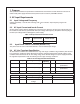
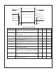
. DC Output Specification 3.1 Output Power / Currents Voltage Table 4: Load Range Minimum Continuous Load Maximum Continuous Load +3.3V 0.5A 25A +5V 0.5A 25A +12V 0.8A 65A -12V 0.1A 0.5A +5VSB 0.1A 3.5A Notes: 1: The +3.3 &+5 Volt total outputs shall not exceed 150W. 2: The maximum output power shall not exceed 800W. 3: Noise bandwidth is from DC to 20 MHz 3.2 Voltage Regulation, Ripple and Noise Table 5: Regulation, ripple and noise Output Voltage +3.
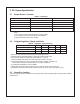
Table 6: Capacitive Loading Conditions 3.4 Output MIN MAX Units +3.3V 10 12,000 uF +5V 10 12,000 uF +12V 10 11,000 uF -12V 1 350 uF +5VSB 1 350 uF Dynamic Loading The output voltages shall remain within the limits specified in Table-Regulation, ripple and noise for the step loading and within the limits specified in Table-Transient Load Requirement for the capacitive loading.
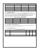
Figure 1: Output Voltage Timing Vout V1 10% Vout V2 V3 V4 Tvout_on Tvout_off Tvout_rise Table 9: Turn On/Off Timing Item Description MIN MAX Units Tsb_on-delay Delay from AC being applied to +5VSB being within regulation. 1500 mS Tac_on-delay Delay from AC being applied to all output voltages being within regulation. 2500 mS Tvout_holdup Time all output voltage stay within regulation after loss of AC tested at 80% of maximum load.
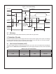
Figure 2: Turn On/Off Timing AC Input AC off AC On Tvout_holdup Vout Tac_on-delay Tpwok_low Tsb_on-delay PWOK Tpwok_on +5VSB Tsb_vout Tpwok_off Tpwok_holdup Tpwok_off Tsb_on-delay Tpwok_on Tpson_pwok Tsb_holdup Min.>70mS Tpson_on_delay PSON# AC turn 0n/off cycle 3.7 PSON turn on/off cycle Efficiency The minimum power supply system efficiency shall be 80% at typical load. 4.
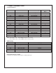
4.2 Over Voltage Protection (OVP) The power supply shall shut down and latch off after an over voltage conditions occurs. Table 11: Over Voltage Protection Voltage Minimum Maximum Shutdown Mode 4.3 +5V +5.7V +6.5V Latch Off +3.3V +3.9V +4.5V Latch Off +12V +13.3V +14.5V Latch Off Short Circuit Protection The power supply shall shut down in latch off mode when the output voltage is short circuit. 4.
5.6 Electromagnetic Compatibility Electromagn etic Interference FCC CFR Title 47 Part 15 Sub Part B EN55022/EN55024 Harmonics IEC61000-3-2 Class D Flicker IEC61000-3-3 ESD Susceptibility EN-61000-4-2 Radiated Susceptibility EN61000-4-3 EFT/Burst EN61000-4-4 Surge Voltage EN61000-4-5 Conducted Susceptibility EN61000-4-6 RF Conducted Voltage Dips and Interruptions Leakage Current 5.
7.
Bit Number 7 6 5 4 3 2 1 0 Status Bit Name Reserved Reserved Reserved Reserved Reserved Module Status PS_ON Status AC Status Device address locations PDB adderss A0/A1 PSU PMBUS Device 0/0 B0h Meaning Default=0 Default=0 Default=0 Default=0 Default=0 Inserted=0, Not inserted=1 PS_OFF=0, PS_ON=1 AC OK=0, AC Fail=1 0/1 B2h 1/0 B4h 8.