
User Manual

SECTION 1: THEORY OF OPERATION
~\Technical Documentation\System Manuals\FCC-Reports\IP8HPV\IP8HPV-FCCRpt.doc Page 6
(870MODE line), it provides a serial interface for the MDT-870. Notice that only the RX data (RXD) and
all handshake lines are buffered. Transmit data (TXD) is derived from a modem interface circuit.
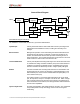
Injection Synthesizer
The synthesizer chip is the major contributor of the injection synthesizer. This device contains the key
components of a phase locked loop (PLL), including a prescaler, programmable divider, and phase
detector. The selected frequencies are loaded into the synthesizer chip as a clocked serial bit stream via
the PLL DATA and PLL CLOCK inputs. The microcontroller provides the serial data.
A 10 MHz reference frequency is provided by voltage controlled, temperature controlled crystal oscillator
module. This device has an input that accepts transmit modulation and voltage from a RX FREQ
ADJUST pot. The pot allows the receiver to be fine-tuned to the exact operating frequency.
The injection signals are generated by a voltage controlled oscillator (VCO) module VCO1 (approximately
850-870 MHz). A voltage on the C input determines the VCO frequency. The voltage is generated by the
phase detector output (PDOUT) of U14 driving a loop filter consisting of R42, C50, C51, and R39. It
integrates the pulses that normally appear on PDOUT into a smooth DC control signal for the VCO. Upon
transmit, the analog signal from the modem and transmit modulation circuitry is applied to VCO1 via the
M input.
The output of VCO1 passes through a high-linear switch (SW3), which is then attenuated by resistors
R114-R116 for improved loop stability, and then amplified by an RF amplifier (U11). From U11 the signal
passes through a two-way divider (U10). One port of U10 passes through another two-way divider (U12).
The first port of U12 provides the receive injection (RXINJ1) signal for Receiver 1, while the second port
output provides the receive injection (RXINJ2) signal for Receiver 2. The other port of U10 passes
through another two-way divider (U13). One port returns to the synthesizer FIN+ input via the VCO
feedback completing the loop signal path. The other port of U13 provides the transmit injection (TXINJ)
signal for the transmitter circuit.
A second VCO module (VCO2) is included for future applications.
Transmitter/TR Switch
The transmitter section consists of an exciter, power amplifier, and power control circuitry. The exciter is
built around an RF power amplifier chip. To transmit, TXKEYOUT* is pulled low. This causes this
amplifier to power up and amplify the TXINJ signal input through a voltage variable absorptive attenuator.
PA12V is also powered up. This causes the power amplifier to boost the RF power to the desired level.
Up to 16 watts are available from the transmitter.
Receiver 1 Front-End
This section consists of the components that form Receiver 1 Front-End. These components include
surface acoustic wave (SAW) filters, a low-noise amplifier, and a mixer.
Incoming signals pass through a low-loss SAW filter that provides a high degree of out-of-band signal
rejection. A low-noise amplifier amplifies the selected signals and another low-loss SAW filter provides
additional selectivity. The output from this low-loss SAW filter connects to a mixer. This mixer is a MMIC
mixer which heterodynes the receive injection signal from the synthesizer. The result is a 45 MHz IF
signal and the IF signal goes through crystal filters (FLT3 and FLT4) to the Receiver 1 IF section for
further processing.