tm INVADR IP1B Base Station Owner’s Manual Date Prepared: April 4, 2002 Document Control #: DC-27 Version: C-2 (Special Release) Copyright 2002 IP MobileNet, Inc.
TABLE OF CONTENTS SECTION 1: THEORY OF OPERATION .................................................................................. 3 General Block Diagram ........................................................................................................... 3 System Control Block Diagram ...................................................................................... 4 Microcontroller Description .................................................................................
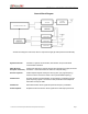
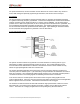
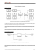
SECTION 1: THEORY OF OPERATION General Block Diagram General block diagram of the IP1B, which is comprised of eight (8) PCBs (Printed Circuit Boards). System Controller Consists of a system microcontroller, radio modem, and provides serial communication interfaces. DRC (Diversity Reception Controller) Continuously selects the receiver with the best signal level to supply recovered modulation. Eliminates destructive effects of multi-path fading.
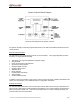
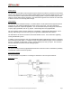
SECTION 1: THEORY OF OPERATION System Controller Block Diagram Functional block diagram of the System Controller. The system controller controls all programmable devices in the radio and handles internal and external communications. Microcontroller Description The base station uses a SGS/Thomson ST10F167 microcontroller.
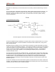
SECTION 1: THEORY OF OPERATION For up-link transmissions, the microcontroller receives data from the receive modem chip, checks for errors, adds framing and optionally signal strength information, and sends it out the serial port. Synthesizers The microcontroller is responsible for keeping the base station on channel by programming the digital PLL (phase-locked-loop) frequency synthesizers.
SECTION 1: THEORY OF OPERATION Carrier Detect The base station uses RSSI (received signal strength indicator) and software to generate a carrier detect signal. Every millisecond, the microcontroller samples RSSI through an analog-to-digital converter. If the microcontroller detects a step increase in the RSSI voltage (greater or equal to the RSSI step threshold setting), a carrier detect signal is generated.
SECTION 1: THEORY OF OPERATION The receiver injection synthesizer creates the injection signals used by the three (3) internal FM receivers. The receiver injection frequency is 45 MHz below the base station’s receive frequency. The VHF signal from the VCO is applied to amplifier for amplification and load isolation and is then routed to a 4-way divider network. The divider network splits the injection signal into four (4) equal amplitude signals.
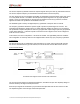
SECTION 1: THEORY OF OPERATION After the final band-pass filter, the signal is applied to a mixer where it is mixed with the receiver injection signal (45 MHz below the received signal) to produce a first IF of 45 MHz. The 45 MHz IF is passed by a 45 MHz crystal filter and is routed to the 45 MHz receiver section for further processing. 45 MHz Receiver Section Functional block diagram of the 45 MHz receiver. The 45 MHz IF from the front-end is mixed with a 44.
SECTION 1: THEORY OF OPERATION Diversity Reception Controller Principle of Operation The DRC is the central processor of a patented triple-receiver DRC. The DRC accepts inputs from three (3) receivers, determines which receiver has the best SNR (signal-tonoise ratio), and selects that receiver to supply recovered modulation. High-speed RSSI from the three (3) receivers are processed by the RSSI input and RSSI level- shifter sections, and are then forwarded to the receiver selector.
SECTION 1: THEORY OF OPERATION DIVAUDIO is routed directly to the internal modem as the modem provides internal filtering of received signals. For an external device, DIVAUDIO is routed through a 4800 Hz eighth-order Bessel low-pass filter. The purpose of the filter is to improve the SNR of the recovered signal. Following the filter, the signal is buffered to provide load isolation and is routed to an external device as FDATA (filtered, diversity recovered modulation).
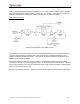
SECTION 1: THEORY OF OPERATION Exciter RF Section Functional block diagram of the exciter RF section. The exciter RF section generates the transmit RF carrier and accomplishes FM modulation. The VHF signal from the VCO is applied to a buffer and is then routed to a divider network. The divider network splits the RF signal into two (2) equal amplitude signals. One of these signals is used as the exciter output; the other is sent back to the synthesizer as feedback for the PLL.
SECTION 2: FCC LABEL FCC Label The following table identifies the information related to FCC label placement for the IP1B. NO. 1 DOCUMENT NO. IP1B-Drawing DESCRIPTION INVADR IP1B Base Station Drawing – FCC Label Placement (1 Page) ~\Technical Documentation\System Manuals\FCC-Reports\IP1B-FCCRpt.
SECTION 2: FCC LABEL IP1B Base Station FCC Label Placement IP1B Base Station FCC Label ς ΗΦ (150−156 ΜΗζ) ΒΑΣΕ ΣΤΑΤΙΟΝ ∗∆Ις ΕΡΣΙΤΨ ΡΕΧΕΠΤΙΟΝ ΣΨΣΤΕΜ ς ΗΦ (150−156ΜΗζ) ΒΑΣΕ ΣΤΑΤΙΟΝ ∗∆Ις ΕΡΣΙΤΨ ΡΕΧΕΠΤΙΟΝ ΣΨΣΤΕΜ ΣΧΑΛΕ : 2Ξ ~\Technical Documentation\System Manuals\FCC-Reports\IP1B-FCCRpt.