IPSeries IP4B Base Station Product Owner’s Manual Date Released: January 20, 2003 Document #: 516-80476-POM Version: A (Special Release) Copyright 2003 IPMobileNet, Inc. .
TABLE OF CONTENTS SECTION 1: THEORY OF OPERATION .................................................................................................... 3 General Block Diagram.................................................................................................................. 3 General Block Diagram Definitions ..................................................................................... 3 Input/Output ......................................................................................
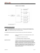
SECTION 1: THEORY OF OPERATION GENERAL BLOCK DIAGRAM General Block Diagram Definitions For increased data security, the modem supports the U.S. Government developed Digital Encryption Standard (DES) data encryption and decryption protocols. This capability requires installation of thirdparty IP compliant DES encryption and decryption software. The standard IPSeries base station circuit board contains five (5) main sections defined below: Input/Output System Controller 298994.
SECTION 1: THEORY OF OPERATION Modems Convert data into an analog audio waveform for transmission and analog audio from the receiver to serial data interface. There is one (1) modem that is dedicated to the transmit operation and two (2) modems dedicated to the receive operation. The modem dedicated to the transmit supports a 115.2 KBPS data transmission rate on the serial port, SLIP protocol, and a 19.2 KBPS OR 9.6 KBPS over-theair data transmission rate.
SECTION 1: THEORY OF OPERATION IP4B Base Station Section Descriptions System Controller This section displays the Central Processing Unit (CPU)(U1), clock, and power-on reset circuitry. It provides more processing power than required for future capabilities to be incorporated without changing processors. Such capabilities include data encryption/decryption (DES) and remote fault monitoring. U1 features a 16-bit address bus and 128K of internal flash random access memory (RAM).
SECTION 1: THEORY OF OPERATION Modem This base station uses separate modems for receive and transmit functions so that full-duplex operation may be obtained. The A0-A1 address bus in addition to the individual read (RD*), write (WR*), and chip select (MODEMTXCS*) lines control all three (3) modems. Modem operations are timed by Y2, a 4.9152 MHz clock module. Modem chip U14 is dedicated to the transmit operation.
SECTION 1: THEORY OF OPERATION Baseband This circuitry amplifies the audio from each receiver, routes it through a RF multiplexer, and selects the audio from the receiver with the highest RSSI value. The comparator circuit on the previous sheet controls it. There are three (3) channels of audio, with separate gain and DC offset adjustments to compensate for performance differences in the receivers. For example, incoming audio from receiver 1 appears at AUDIO 1. An op amp (U12D) is then amplifies the audio.
SECTION 1: THEORY OF OPERATION Receiver Injection This displays a serial data input/output interface, synthesizer, and VCO. The I/O interface circuitry accepts clock, serial data, and enable signals from the System Controller Board via terminal block TB1. A lock detect (LD) status output is returned to the System Controller Board from the synthesizer. U3 is a hex Schmidt Trigger inverter, which squares up incoming signals for reliable operation of the synthesizer chip.
SECTION 1: THEORY OF OPERATION A regulator (VR2) powers the T/R switch circuitry. When the System Controller Board makes TXKEY* low, inverter U6D goes high, turning on transistor Q2 and FET Q1. This applies 5-volt power to the TXENABLE output, turning on the T/R switch on the Power Amplifier Board. At the same time, transistor Q3 conducts, grounding the KEY* input of the Power Amplifier Board.
SECTION 1: THEORY OF OPERATION input determines the VCO frequency. The voltage is generated by the phase detector output (PD/O) of U2, which drives a loop filter consisting of R19, C16, C17, and C47. The filter integrates the pulses, which normally appear on PDOUT into a smooth DC control signal for the VCO. The output of VCO1 is attenuated by module AT2, resulting in improved VCO stability. Amplifier U8 amplifies the signal and applies it to a splitter (U3). One output of U3 is connected to a switch (U1).
SECTION 2: FACTORY TEST PROCEDURE Equipment List The following table lists the equipment required to perform the IP4B Base Station Factory Test Procedure. CHECKLIST OF REQUIRED MATERIAL FOR PRELIMINARY TESTING OF THE IPSeries BASE STATION NO.
SECTION 2: FACTORY TEST PROCEDURE Programming and Configuring the Base Station This section applies to all frequency ranges of the IPSeries Base Station. Important! The base station’s IP address must be known prior to performing the procedures in this section. The programming procedure should be performed when it is necessary to upgrade a base station’s Firmware or to change the operating parameters to suit client needs.
SECTION 2: FACTORY TEST PROCEDURE Adjustment / Alignment Procedures Make appropriate notations of any items that require attention during this procedure. This information is needed later during the repair process. Startup Step 1 Remove the base station cover placing the screws in a location where they will not be misplaced. Step 2 Connect the base station to the appropriate components. Step 3 Power up the base station and computer. The power supply ammeter must read 1.2 amps or less with a 13.
SECTION 2: FACTORY TEST PROCEDURE Diversity Reception Step 1 Inject an on-frequency signal at a level equal to Receiver 1 12dB SINAD level, modulated with a 1 KHz test tone at ±5.0 KHz deviation into Receiver 1. Step 2 While monitoring TP1 with the digital multi-meter, adjust RSSI1 low adjust potentiometer (R12) for a reading of 0.750 VDC ±10 mV. Step 3 Increase the amplitude of the signal by 50 dBm.
SECTION 2: FACTORY TEST PROCEDURE Step 13 Inject on-frequency signal at a level of –80 dBm, modulated with a 1 KHz test tone at ±5.0 KHz deviation into Receiver 1. Step 14 While monitoring the AC voltage at TP6 adjust audio 1 AC adjustment potentiometer (R72) for 350 mVRMS (±1 mV). Step 15 While monitoring the DC voltage at TP6 adjust audio 1 DC adjustment potentiometer (R57) for 2.500 VDC (±1 mV).
SECTION 2: FACTORY TEST PROCEDURE Exciter Step 1 Using the X=1400,19 command, generate data messages so the transmit power and frequency can be checked. Step 2 Note the power level and then on the power amplifier circuit board adjust the potentiometer (R3) fully counterclockwise (this will enable low power transmit operation). Step 3 Connect the base stations’ transmit port to the HP communication test set.
SECTION 3: FCC LABEL IP4B Base Station FCC Label Placement IP4B Base Station FCC Label MUST BE SUITABLE FOR TYPING. 400-512MHz BASE STATION Serial No. Model: IP4B U.S. PATENT Nos. 5.640.695, 6,018,647, 6,243,393 Made in U.S.A. SCALE : 2X 400-512MHz BASE STATION Serial No. Model: IP4B 298994.DOC U.S. PATENT Nos. 5.640.695, 6,018,647, 6,243,393 Made in U.S.A.
APPENDIX A: CIRCUIT BOARD DIAGRAMS System Controller J2 32 Y1 C76 25 26 C84 1 U13 R80 100 C74 J3 R79 16 U2 R50 R62 R65 50 109 51 C56 108 T1 R66 C83 76 C75 R51 75 C77 S3 C8 REWORK INSTRUCTION ADD JUMPER (30 AWG INSULATED WIRE) from U19 Pin2 to VIA (RVCC) U10 S2 J1 C7 R33 C28 U14 R31 U8 TP5 73 72 U19 U18 C58 R88 C59 R83 R82 R81 U20 + U17 D7 U7 C90 8 U21 S1 U15 U4 U6 TP8 7 J5 C88 R43 1 R44 R41 12 R42 R39 R40 J8 C89 1 J7 VR3 9 1 10 2 TP4 Y2 F1 U16
APPENDIX A: CIRCUIT BOARD DIAGRAMS Receiver – Bottom Receiver Injection TB1 VR1 C51 R26 C50 + C52 + C54 VR2 C53 C49 C32 C33 VCO1 C26 AT1 C46 + C31 L1 U8 C30 C29 C34 R3 C2 R16 C28 R17 JMP1 1 U5 U6 R5 R25 C20 R21 C21 CR3 U7 C10 U3 R8 C1 C19 + R4 C16 U2 C3 + + C5 C6 L2 C36 C4 C37 C14 + C35 C12 P3 298994.
APPENDIX A: CIRCUIT BOARD DIAGRAMS Exciter – Top Exciter – Bottom 298994.
APPENDIX A: CIRCUIT BOARD DIAGRAMS Power Amplifier + 298994.
APPENDIX B: IP4B TEST DATA SHEET Program and Configure the Base Station Date Serial Number Firmware Revision End User Tester Adjustment / Alignment Procedures Receiver Injection Parameter Spec Injection Frequency Error at RXINJ1(within +/- 10 Hz of exact injection frequency) P1 & C39 Measured +/- 100 Hz 5 +/- 1 dBm Receiver Diversity Reception Controller 1, 2 & 3 Parameter Spec U6 Pin 4 +10 to +5 dBm RSSI Test Point TB1-4 2.8 to 3.0 VDC Distortion (1 kHz Test Tone @ 5.
APPENDIX B: IP4B TEST DATA SHEET Data Quality Parameter Spec Receiver 1 Data Quality (x=1400, 19 Command IPMessage Utility) 240> Receiver 2 Data Quality (x=1400, 19 Command IPMessage Utility) 240> Receiver 3 Data Quality (x=1400, 19 Command IPMessage Utility) 240> Measured Exciter Parameter Spec Transmit Frequency Error (Transmitting 1400 character test message) Transmit Modulation Deviation (5.