
User's Manual


FCC ID: MI7-ECSHPA80TX
A9
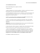
Sheet 4 of 6.
RF input, driver, and power divider circuitry. The purpose of this circuitry
is to attenuate the incoming RF energy, amplify it to a useful level, and to divide it into
four equal parts for the power amplifier modules. This design approach allows the HPA8
to accept a wider range of RF power levels than otherwise possible.
The RF input circuitry is built around coupler DC1 and adjustable attenuator AT1. In
operation, RF energy from the IP8B Base Station Data Transceiver appears at the RF IN
pad. Coupler DC1 reduces the RF signal level by 75%, courtesy of resistors R26 and
R30. The RF is sent to the attenuator via capacitor C16. DC controlled attenuator AT1
adjusts the RF power level for the desired output (typically 80 watts). Pot R25 controls
the attenuator. Capacitor C17 couples the RF output to the driver circuitry.
The driver circuitry consists of amplifier U6. This device boosts the RF signal from
attenuator AT1 to up to one watt of RF power. Amplifier U6 is operated by a 8 volt
regulated source and a DC control input from sheet 3. To transmit, the 5VKEY input is
made high and amplifier U6 becomes active. This produces an RF output on pin 13.
From there the RF goes through a PI filter consisting of capacitors C20/C21 and choke
L1. The filter provides harmonic suppression and impedance transformation for the
couplers in the power divider section. Chokes L2 and L3 provide a DC path for the
circuitry inside of U6, while capacitor C22 blocks DC from the RF before it goes to the
power dividers.
The power divider circuitry consists of three hybrid couplers. The purpose of these
devices is to divide the RF power output into four equal parts. Coupler HC3 accepts RF
from the driver, and it produces outputs at 0
o
and –90
o
. Coupler HC1 is driven by the 0
o
port of HC3. It produces RF outputs at 0
o
and –90
o
for the first two power amplifier
modules. Coupler HC2 is driven by the -90
o
port of HC3. It produces RF outputs at -90
o
and –180
o
for the second pair of power amplifier modules.
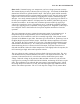
Sheet 5 of 6.
Power amplifier modules. The four hybrid power amplifier modules are
shown here. The devices are powered through FET switches on sheet 3 via VS1 and
VS2. The four modules are biased for class AB operation via VBB. This voltage is
developed by an adjustable voltage regulator on sheet 3.
Should a power amplifier module fail, a portion of the power is lost. As a result, the
power output drops from 80 watts to 60 watts. Should a second power amplifier module
fail, the power output drops from 80 watts to 40 watts for the same reason. This is the
“graceful degradation of power under fault conditions” concept in operation.