
User's Manual
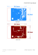
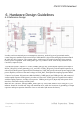
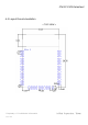
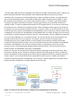
Table Of Contents

Proprietary & Confidential Information
iotTech Corporation, Taiwan
Doc. NO:
ITM-FCC3F1 Datasheet
6. Hardware Design Guidelines
6-1 Reference Design
In order to achieve minimal power consumption, users may, under all types of operational modes,
control the power modules in the control chip in OPL1000A2 chip of internal high-performance Buck
& LDO DC-DC Converter. The system power, with input of decoupled capacitor from external
battery power originated from VDD_BAT (pin 15), reduces noise with in-chip Buck DC-DC
Converter, respectively in,
1.
RF Power System: output of 1.3 VDC at SMPS_RF (pin 18), via decoupled capacitor, then
input at
DCDC_IN (pin 5), before generating 1.1V, via LDO, at VDD_RF (pin 6), with decoupled capacitor, in
order to provide the power required by RF. Furthermore, VDD_PA
(pin 9) is the main power supply of PA
power amplifier, which is of the same voltage as VDD_BAT, and requires decoupling capacitor added.
2.
Inner-Core System: PI circuits are added at SMPS_CORE (pin 19) and VDD (pin 20), and connected
via decoupled capacitor VDD (pin 41), in order to lower noise. VDDC (pin 10 is required to be added
with decoupling capacitor, in order to lower noise. VDDO (pin 26, pin 35, & pin 43) is the power for IO
interface, of the same voltage as VDD_BAT.
Buck DC-DC converter, through SMPS_IND1 (pin 16), series with inductor L2 to FB (pin 17), as
inductor should be located near chip with minimum area, while the locations of grounding of output
capacitor and input capacitor should be close to each other (the nearer the better).