
Users Manual
ISM14585-EVB User’s Manual
DOC-DS-14585-EVB-201911-3.6
Confidential Inventek Systems
Page 5
additional cost. The wide supply voltage range (0.9 –3.6 V) covering a larger choice of energy
sources also enables full design flexibility.
The ISM14585-L35 is easy to design-in and supports standalone as well as hosted
applications. The ISM14585-L35 is supported by a complete development environment with
Dialog’s SmartSnippets™ software that helps customers optimize software for power
consumption.
The ISM14585-L35 supports several fully qualified profiles embedded in ROM (see “Typical
Applications” below), and the option of loading additional profiles into RAM. The low cost,
small foot print (6.0mm x 8.6mm x 1.2mm), LGA 35 pin package and ease of design-in make
the ISM14585-L35 ideal for a wide range of embedded applications.
The ISM14585-L35 enables wireless connectivity to the simplest existing sensor products
with minimal engineering effort. ISM14585-L35 reduces development time, lowers
manufacturing costs, saves board space, simplifies certification compliance, and minimizes
customer RF expertise required during development of target applications.
The ISM14585-L35 provides the highest level of integration for a wireless system, with market
leading and integrated BLE 5.0 technology based on Dialog’s DA14585 SoC.
The ISM14585-L35 is also fully supported by Dialog’s Smartbond product family Development
Kit-Pro evaluation board and Dialog SmartSnippets Studio SDK.
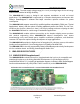
3 ISM14585-EVB FEATURES
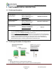
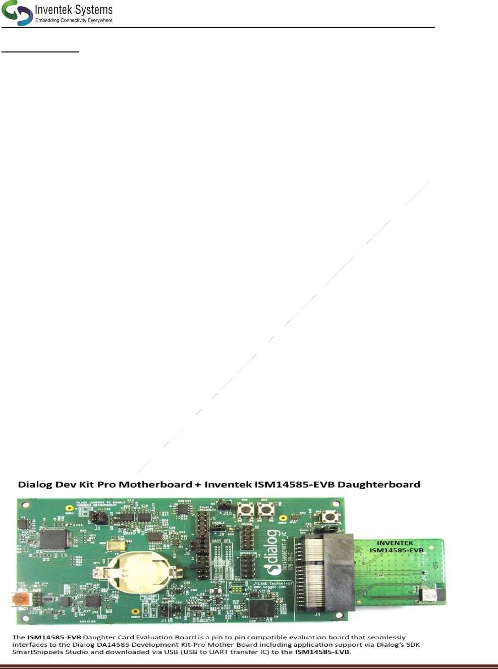
3.1 ISM14585-EVB Daughterboard
The ISM14585-EVB evaluation board is a Daughterboard that is pin to pin compatible and
seamlessly interfaces to the Dialog DA14585 Development Kit-Pro Motherboard (P/N
DA14585-00ATDEVKT-P), including all application support via Dialog’s SDK SmartSnippets
Studio and downloaded via USB (USB to UART transfer IC) to the ISM14585-EVB.