Service Manual CK30 Handheld Computer
Intermec Technologies Corporation Corporate Headquarters 6001 36th Ave. W. Everett, WA 98203 U.S.A. www.intermec.com The information contained herein is proprietary and is provided solely for the purpose of allowing customers to operate and service Intermec-manufactured equipment and is not to be released, reproduced, or used for any other purpose without written permission of Intermec.
Contents Contents Before You Begin ............................................................................................................. vii Safety Summary .................................................................................................. vii Safety Icons........................................................................................................ viii Global Services and Support.................................................................................
Contents IT4000 Imager Assembly Exploded View......................................................................... 35 IT4000 Imager Assembly Spare Parts List ........................................................................ 35 Tethered Scan Flex Assembly Exploded View................................................................... 36 Tethered Scan Flex Assembly Spare Parts List................................................................... 36 Safety Labels Exploded View ..................
Contents Display Contrast Control.................................................................................... 66 Temperature Compensation................................................................................ 67 Backlight............................................................................................................. 67 Keypad............................................................................................................................. 67 Key Matrix Scanning......
Contents AC1 4-Slot Battery Charger .............................................................................. 101 AC2 4-Bay Charging Dock ...............................................................................
Before You Begin Before You Begin This section provides you with safety information, technical support information, and sources for additional product information. Safety Summary Your safety is extremely important. Read and follow all warnings and cautions in this document before handling and operating Intermec equipment. You can be seriously injured, and equipment and data can be damaged if you do not follow the safety warnings and cautions.
Before You Begin Safety Icons This section explains how to identify and understand dangers, warnings, cautions, and notes that are in this document. You may also see icons that tell you when to follow ESD procedures and when to take special precautions for handling optical parts. A warning alerts you of an operating procedure, practice, condition, or statement that must be strictly observed to avoid death or serious injury to the persons working on the equipment.
Before You Begin Global Services and Support Warranty Information To understand the warranty for your Intermec product, visit the Intermec web site at http://www.intermec.com, click Support, and then click Warranty. Disclaimer of warranties: The sample code included in this document is presented for reference only. The code does not necessarily represent complete, tested programs. The code is provided “as is with all faults.
Before You Begin Who Should Read This Document? This manual contains all of the information necessary to repair the CK30 handheld computer. It provides an exploded view of the computer, the spare parts lists, procedures that describe how to replace parts, and information about how to test the computer. This manual is written for service technicians.
1 Troubleshooting Use this chapter to troubleshoot problems you may encounter while using the CK30.
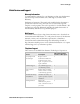
Chapter 1 — Troubleshooting Troubleshooting the CK30 Use this table to find common problems users may experience with their CK30 and possible solutions. Problem You press I to turn on the CK30 and nothing happens. Solution Try these possible solutions in order: • Make sure you have a charged battery installed correctly. For help, see “Charging and Installing the Battery” in the CK30 Handheld Computer User’s Manual (P/N 073528).
Chapter 1 — Troubleshooting Troubleshooting the CK30 (continued) Problem Nothing is displayed on the screen. Solution Try these possible solutions in order: • The contrast may be set too light or too dark. Press B and then E repeatedly until you reach the desired contrast level. • If you have a CK30 with a color screen, make sure the backlight is on by pressing E. • The display flex cable may be disconnected. Make sure the display flex cable is connected to the display assembly and the main PCB.
Chapter 1 — Troubleshooting Troubleshooting the CK30 (continued) Problem The CK30 will not communicate in a serial network. Solution Try these possible solutions in order: • The CK30 may not be properly configured for serial communications. Make sure the serial communications parameters are properly configured. • The AA1 serial adapter cable may have failed. Replace the serial adapter cable. • The main PCB assembly serial interface may have failed.
Chapter 1 — Troubleshooting Troubleshooting the CK30 (continued) Problem The CK30 will not communicate in a wireless network. Solution Try these possible solutions in order: • Make sure that the radio is configured properly for the network. If the radio is properly configured, there may be a problem with the access point. • Make sure that the antenna cables are correctly connected to the radio. If the antenna cables are correctly connected, the antenna or radio may be damaged.
Chapter 1 — Troubleshooting Troubleshooting the CK30 (continued) Problem The CK30 cold boots or loses settings after the main battery is replaced. Solution Try these possible solutions in order: • Make sure the main battery is fully charged. • The bridge battery or the power circuitry on the main PCB may be faulty. For help, see the “Replacing the Main PCB” procedure on page 15. The CK30 cannot communicate with a Bluetooth printer.
2 Replacing Parts Use this chapter to learn how to open, replace parts in, and close the CK30 handheld computer. It also provides preliminary cautions to follow when servicing the CK30.
Chapter 2 — Replacing Parts Cautions Note: Opening this product can result in voiding the warranty. The internal workings of this product can only be accessed by Intermec service personnel. Integrated circuits on the printed circuit board (PCB) in the computer are very sensitive to damage by electrostatic discharge (ESD). Prevent ESD by always wearing skin contact ground straps firmly attached to the equipment metal base assembly when working inside of the computer.
Chapter 2 — Replacing Parts Replacing Parts This section describes how to open, replace parts in, and close the CK30 handheld computer. Each procedure also lists the tools and parts that you will need. Opening the CK30 To replace the internal parts of the CK30, you need to open it. To open the computer, you need the following tools: • T10 Torx screwdriver • Small Phillips screwdriver • Phillips 2-56 x .312 screw (P/N 590371-001) • Torx 4-40 x .25 machine screw (P/N 590870-001) • Torx 4-20 x .
Chapter 2 — Replacing Parts 5 Remove the scanner or imager flex cable from the main PCB. 6 Disconnect the trigger reed switch cable from J4 on the main PCB. The top and bottom covers are now separated. J4 Scanner or imager flex cable Trigger reed switch cable 7 Lay both covers down so that the exterior sides face down. Replacing the 802.
Chapter 2 — Replacing Parts Screw (2 places) Antenna Antenna ground plane Screw (2 places) Screw (2 places) Mini PCI shield assembly Mini PCI radio assembly Bottom cover Retainer clips 4 Use the antenna cable remover tool to carefully lift the antenna off of the mini PCI radio assembly. Insert the prongs under the antenna cable socket and lift gently. Note: Do not pull on the wire because the cable will break.
Chapter 2 — Replacing Parts Replacing the Ethernet Card To replace the Ethernet card, you may need the following tools and parts: • T10 Torx screwdriver • Small Phillips screwdriver • Ethernet card assembly (P/N 073867-001) • Ethernet cable assembly (P/N 073096-001) • 2-56 x 3/16 stainless steel screw (P/N 801-210-000) • 2-28 x .250 Plastite flathead screw (P/N 800-193-000) To replace the Ethernet card 1 Open the CK30. For help, see “Opening the CK30” on page 9.
Chapter 2 — Replacing Parts 6 Replace the mini PCI shield assembly by threading the Ethernet cable through the opening in the shield and replacing the four Phillips screws. 7 Connect the Ethernet cable to J12 on the main PCB. 8 Close the CK30. For help, see “Closing the CK30” on page 27. Replacing the Bluetooth Radio To replace the Bluetooth radio, you need the following tools and parts: • T10 Torx screwdriver • Small Phillips screwdriver • Bluetooth radio (P/N 855-050-001) • Phillips 4-40 x .
Chapter 2 — Replacing Parts Screw (1 place) Bluetooth radio retaining clip Bluetooth radio module Screw (2 places) Flip main PCB over to access Bluetooth radio Display flex cable Keypad flex cable 6 Lift up on the Bluetooth radio module and remove it from the main PCB. 7 Replace the Bluetooth radio module. 8 Replace the Phillips screw that attaches the Bluetooth radio retaining clip to the main PCB. 9 Connect the display flex cable and the keypad flex cable to the main PCB.
Chapter 2 — Replacing Parts Replacing the Main PCB To replace the main PCB, you need the following tools: • T10 Torx screwdriver • Small Phillips screwdriver You also need one of the following parts depending on the CK30 configuration: • CK30 64M/64M main PCB assembly (P/N 072291S-007) • CK30 32M/32M main PCB assembly (P/N 072926S-008) • LCD support bar (P/N 073497-002) • KA22 x 6 WN 1412 Elco screw (591825-001) To replace the main PCB 1 Open the CK30. For help, see “Opening the CK30” on page 9.
Chapter 2 — Replacing Parts Screw (2 places) Display flex cable Keypad flex cable 6 Remove the Bluetooth radio (if necessary). For help, see “Replacing the Bluetooth Radio” on page 13. 7 Attach the new LCD support bar to the new main PCB. LCD support bar 8 (If necessary) Replace the Bluetooth radio. 9 Attach the display flex cable and keypad flex cable to the main PCB. 10 Insert the main PCB into the top cover and replace the two Phillips screws at the top of the main PCB.
Chapter 2 — Replacing Parts Replacing the Bezel Assembly To replace the bezel assembly, you need one of the following parts depending on the CK30 configuration: • CK30 programmable 42-key bezel assembly (P/N 073297-001) • CK30 international 42-key bezel assembly (P/N 073298-001) • CK30 3270/5250 42-key bezel assembly (P/N 073299-001) • CK30 ANSI 42-key bezel assembly (P/N 073300-001) • CK30 programmable 50-key bezel assembly (P/N 073293-001) • CK30 international 50-key bezel assembly (P/N 073294-001) • CK3
Chapter 2 — Replacing Parts 4 Once a corner of the bezel is loose, gently pull up on the bezel to remove it. 5 Remove the adhesive residue left on the top cover from the bezel assembly. 6 Separate the adhesive strip from the back of your new bezel assembly. 7 Insert the keypad bezel end of the assembly, snap it into place, and then press down firmly on the overlay surrounding the display to attach the bezel assembly to the CK30 top cover.
Chapter 2 — Replacing Parts Screw (2 places) Display flex cable Keypad flex cable 5 Lift the display assembly away from the top cover. 6 Remove the power indicator/good read light pipe assembly and the speaker PCB assembly. (If necessary) Remove and replace the user indicator light pipe assembly. 7 Attach the power indicator/good read light pipe assembly and the speaker PCB assembly to the new display assembly.
Chapter 2 — Replacing Parts 8 Insert the new display assembly into the top cover. 9 Attach the display flex cable and the keypad flex cable to the main PCB. 10 Replace the main PCB and secure it with the two Phillips screws removed in Step 3. 11 Connect the power indicator/good read light pipe assembly cable and the speaker PCB cable to the main PCB. 12 Close the CK30. For help, see “Closing the CK30” on page 27.
Chapter 2 — Replacing Parts Keypad assembly Keypad flex cable 4 Remove the adhesive residue left by the keypad assembly on the top cover. 5 Remove the adhesive backing from the new keypad assembly. Keypad assembly Adhesive backing 6 Connect the keypad flex cable to the keypad assembly and firmly attach the keypad assembly to the top cover. Make sure the keypad flex cable properly z-folds under the main PCB. 7 Insert a new bezel assembly. For help, see “Replacing the Bezel Assembly” on page 17.
Chapter 2 — Replacing Parts To replace the SE1200 scanner 1 Open the CK30. For help, see “Opening the CK30” on page 9. 2 From the bottom cover, remove the four Phillips screws that attach the scan engine assembly. 3 Lift the scan engine assembly away from the bottom cover. Screw (4 places) SE1200 scan engine assembly Large scan mount bracket Screw (2 places) 4 Turn the scan engine assembly over and remove the two Phillips screws that attach the scan engine to the large scan mount bracket.
Chapter 2 — Replacing Parts SE1200 scan flex engine Visor Shield Large scan mount bracket Screw (2 places) 7 Insert the scan engine in the scan mount bracket and attach it with the two Phillips screws removed in Step 4. 8 Insert the scan engine assembly into the bottom cover and attach with the four Phillips screws removed in Step 2. 9 Close the CK30. For help, see “Closing the CK30” on page 27.
Chapter 2 — Replacing Parts 4 Turn the scan engine assembly over and remove the two Phillips screws that attach the scan engine and ground spring to the small scan mount bracket. 5 Disconnect the scan flex cable from the scan engine assembly.
Chapter 2 — Replacing Parts Replacing the IT4000 Imager To replace the IT4000 imager, you need the following tools and parts: • T10 Torx screwdriver • Small Phillips screwdriver • IT4000 imager assembly (P/N 073416S-001) • Phillips 4-20 x .250 thread-form screw (P/N 525023) To replace the IT4000 imager 1 Open the CK30. For help, see “Opening the CK30” on page 9. 2 From the bottom cover, remove the three Phillips screws that attach the IT4000 imager assembly.
Chapter 2 — Replacing Parts You also need one or more of the following parts depending on what you need to replace: • Tethered scan flex assembly (P/N 072786-004) • Tethered scanner door (P/N 073366-001) • Tethered scanner cover (P/N 073179-001) • Phillips 2-56 x 3/16 steel screw (P/N 591884-001) • Phillips 2-28 x .250 thread-form screw (P/N 525301) To replace the tethered scanner 1 Open the CK30. For help, see “Opening the CK30” on page 9.
Chapter 2 — Replacing Parts Tethered scanner door b Insert a new tethered scanner door and snap it in place. 6 Insert a new tethered scan flex assembly into the mounting bracket and attach it with the two screws removed in Step 4. 7 Insert the tethered scan flex assembly into the bottom cover and attach it with the four screws removed in Step 2. 8 Close the CK30. For help, see the next procedure, “Closing the CK30.
Chapter 2 — Replacing Parts 4 Replace the six Torx screws (four self-tapping and two machine) and tighten to 9 in-lb. 5 Replace the four Phillips screws and tighten to 2 to 3 in-lb. Screw (4 places) Screw (2 places) Screw (2 places) Screw (2 places) 6 While holding the CK30 in one hand, insert the tabs on the bottom of the battery into the CK30 and snap the battery into place.
3 Spare Parts List and Exploded Views This chapter provides the exploded views and spare parts list for the CK30A, CK30B, and CK30C handheld computers.
Chapter 3 — Spare Parts List and Exploded Views CK30 Exploded View This exploded view contains parts for the 802.11b/g radio version of the CK30. To identify a part, find the part in the exploded view and locate its callout in the following spare parts list. See “Ethernet Card Assembly Exploded View” for Ethernet parts. For exploded views of the EV10, SE1200, IT4000, and tethered scan engines, see the sections later in this chapter.
Chapter 3 — Spare Parts List and Exploded Views CK30 Spare Parts List To identify a part, find the callout in this list and locate the part in the previous exploded view.
Chapter 3 — Spare Parts List and Exploded Views Ethernet Card Assembly Exploded View This illustration shows an exploded view of the Ethernet card assembly. To identify a part, find the part in the exploded view and locate its callout in the following spare parts list. The Ethernet card is only available on the CK30A. Screw (2 places) 1 Screw (2 places) 2 3 Ethernet Card Assembly Spare Parts List To identify a part, find the callout in this list and locate the part in the previous exploded view.
Chapter 3 — Spare Parts List and Exploded Views SE1200 Scan Engine Assembly Exploded View This illustration shows the SE1200 scan engine assembly in relation to the bottom cover. To identify a part, find the part in the exploded view and locate its callout in the following spare parts list. 2 1 6 5 Screw (4 places) 3 Screw (2 places) 4 SE1200 Scan Engine Assembly Spare Parts List To identify a part, find the callout in this list and locate the part in the previous exploded view.
Chapter 3 — Spare Parts List and Exploded Views EV10 Scan Engine Assembly Exploded View This illustration shows the EV10 scan engine assembly in relation to the bottom cover. To identify a part, find the part in the exploded view and locate its callout in the following spare parts list. 1 2 6 3 Screw (3 places) 4 Screw (2 places) 5 EV10 Scan Engine Assembly Spare Parts List To identify a part, find the callout in this list and locate the part in the previous exploded view.
Chapter 3 — Spare Parts List and Exploded Views IT4000 Imager Assembly Exploded View This illustration shows the IT4000 imager assembly in relation to the bottom cover. To identify a part, find the part in the exploded view and locate its callout in the following spare parts list. Screw (3 places) 1 2 IT4000 Imager Assembly Spare Parts List To identify a part, find the callout in this list and locate the part in the previous exploded view.
Chapter 3 — Spare Parts List and Exploded Views Tethered Scan Flex Assembly Exploded View This illustration shows the tethered scan flex assembly in relation to the bottom cover. To identify a part, find the part in the exploded view and locate its callout in the following spare parts list. Screw (2 places) 1 Screw (4 places) 2 4 3 Tethered Scan Flex Assembly Spare Parts List To identify a part, find the callout in this list and locate the part in the previous exploded view.
Chapter 3 — Spare Parts List and Exploded Views Safety Labels Exploded View This illustration shows the location of the safety labels. To identify a part, find the part in the exploded view and locate its callout in the following spare parts list. 2 1 3 4 5 Safety Labels Spare Parts List To identify a part, find the callout number in this list and locate the part in the previous exploded view.
Chapter 3 — Spare Parts List and Exploded Views 38 CK30 Handheld Computer Service Manual
4 Theory of Operation This chapter provides the theory of operation for the CK30 handheld computers and its supporting accessories.
Chapter 4 — Theory of Operation System Architecture The CK30 platform is a 32-bit 3.3V system, with the processor and FPGA cores running at 1.3V and 2.5V, respectively. The design is contained on a single main PCB, except for the following modules: • The keypad is a separate, replaceable module that attaches to the exterior of the product, connected to the main PCB through a flex cable. • The LCD and drivers are contained within a separate display module, connected to the main PCB through a flex cable.
Chapter 4 — Theory of Operation Processor Core Processor The CK30 platform is built around the Intel PXA255 “Cotulla” XScale processor (U1). The low-end configurations of the CK30 (CK30AA and CK30BA) use a 200MHz version of the PXA250 for cost reasons. The high-end configuration (CK30CA) uses a 400MHz version of the part. Refer to Intel documentation for detailed information on the PXA255 XScale processor operation and features.
Chapter 4 — Theory of Operation FPGA_CLK 49.77MHz. Enabled immediately before FPGA download. FPGA_CLK serves both the scanner interface and Mini PCI bridge resident in the FPGA. Audio Codec sampling in computers equipped with audio is based on the audio codec local 24.576MHz oscillator. Memory RAM U6 and U7 constitute the system RAM: 32MBs for the CK30AA and CK30BA, and 64MBs for the CK30CA. The SDRAM is interfaced at 3.3V bus levels through the PXA255 memory controller, at 99.
Chapter 4 — Theory of Operation I/O Signals Platform-specific peripheral control input and output signals are implemented through PXA255 GPIO pins, FPGA (U8) I/O pins, and through HCR registers U11 and U16. In general, signals are assigned among these devices according to these criteria: PXA255 outputs: Used for signals that must hold their state through Suspend, and should not immediately be disabled on a critically low battery event.
Chapter 4 — Theory of Operation PXA255 GPIO Signal Descriptions (continued) PXA255 GPIO Can wake processor from Sleep state. GP2 Function Signal Description Usage BT_WAKEUP* System resume interrupt from Bluetooth module. PXA255 input This is a maskable resume source (See Note 1). Enabled when you select system wakeup from Bluetooth wakeup event. ↓ = interrupt PXA255 input ↑ = interrupt GP3 HOST_DETECT System resume interrupt from USB or dock serial interface.
Chapter 4 — Theory of Operation PXA255 GPIO Signal Descriptions (continued) PXA255 GPIO Function Signal Description Usage GP32 -SDMMC_WP SD slot write protect GP38 -HCR_OE GP48 -POE/PCI_IRQ GP66 KEY_DRV0 HCR registers output enable. This signal floats high on cold boot so that HCR register outputs float to their default-off states (through pull-up and pull-down resistors). Once software has initialized the HCR registers, software should enable the HCR outputs by setting this bit low.
Chapter 4 — Theory of Operation HCR Output Signal Descriptions (continued) HCR Bit Function Signal Description Usage U16 20 CF_RESET Compact Flash slot 0 Reset (unused in CK30). 0 = idle 1 = reset U16 21 USB_EN Enables pull-up on USB bus to acknowledge host and start communications. This can be used to hold off USB communications until the USB driver is ready, or to disconnect a USB session in progress (simulated cable disconnect).
Chapter 4 — Theory of Operation FPGA IO Signal Descriptions Function Signal Description Usage VOL0 Beep volume control 000 = lowest volume 111 = highest volume Scan_LED Scanner Good Read LED 0 = LED off 1 = LED on Scan_LED_High Good Read LED intensity control 0 = low intensity 1 = high intensity User_LED1 User LED1 control 0 = LED off 1 = LED on User_LED2 User LED2 control 0 = LED off 1 = LED on VOL1 VOL2 I2C Bus The I2C bus is used for power management functions and for control of the 2
Chapter 4 — Theory of Operation Bus I/F Scanner I/F SDBUF_D7..0 DMA BUFFER FIFO SA25..0 SCAN_DREQ Host CPU I/F DQM3..
Chapter 4 — Theory of Operation The loader then writes byte values to the FPGA, with write strobe PWE* serving as the CCLK download clock. The FPGA IO is nominally Hi-Z during download. When the download is complete, the FPGA enables its outputs. When its internal DLLs have locked, it raises its DONE output (alternate function of signal SCAN_IRQ*) to signal the download was successful. Software then initializes the FPGA internal register settings.
Chapter 4 — Theory of Operation Software is responsible for shutting off FPGA core power in a critical battery situation. If FPGA power is still on when the system suspends, it will be shut off in hardware by the “Type 2” interlock mechanism described in “Device Power Control” on page 58. FPGA Bus Interface The FPGA occupies PXA255 memory areas 2 and 5 (chip selects HCR/PCI_CS* and FPGA_CS*). Both chip selects are set up as Variable Latency IO areas.
Chapter 4 — Theory of Operation Power System Architecture, Power Supplies +5 V to Status LEDs Vbatt_wall from Battery Pack + 5 Volt Regulator PWR_EN Cur. Iimited Switch Teth Scan Vcc DOCK_EN Cur. Iimited Switch Scan + 5 Volts SCAN_PWR_EN + 3.3 Volt Regulator Cur. Iimited Switch Cur. Iimited Switch AUDIO_5 V LDO Scan 3.3 Volts PCI_3.3 Volts CF_PWR_EN 3.
Chapter 4 — Theory of Operation Power Supplies and Capacities Load CPU core supply VDC 1.30V Capacity .5A Regulator U45 Buck switcher from 3.3 VDC VCCN and VCCkp 3.3V .2A System 3.3V (U39 from main battery, or U44 from supercap) PLL_VCC 1.3V .03A Filtered CPU core supply Core logic, memory IO, and ATT_VCC 3.3V .1A System 3.3V (U39 from main battery, or U44 from supercap) Memory core 3.3V .4A System 3.3V (U39 from main battery, or U44 from supercap) SD slot 3.3V 1.
Chapter 4 — Theory of Operation The charging current is applied through the contacts on the base of the battery; the 26-pin dock connector is not used for charging. See “AD1 Charging” on page 99 for details on the charging circuit in the dock. Supercap A 10-farad 2.5V supercap (C89) provides backup current to hold the machine state while the main battery is being replaced.
Chapter 4 — Theory of Operation Data, Addr WinCE Power Manager Addr, Data Bus Shutdn Intermec Battery Manager GPIO I2C driver Shutdn Devices INT Handler Gates Reset_Out BATT_FAULT Reset_In VDD_FAULT PWR_EN PXA250-based System Memory-mapped Registers Power Management Architecture Wakeup Low Batt Detect Power Supply Controller IO Key Rst SW Low 3.3V Detect Battery, Supercap, Temperature Monitoring I2C Power Switches Enables Super cap Power Supplies Core 1.3V, 3.3V, etc.
Chapter 4 — Theory of Operation System Hardware Power States Power Consumption System Power States Off OS Power States N/A Processor Power States N/A (Typical at 8V) (Maximum at 8V) Notes, Conditions N/A N/A Main battery out, supercap fully depleted. Suspend Suspend Sleep 2mA <3mA Supercap fully charged. If the supercap is depleted, this current can be as high as 70mA. As the supercap charges, this current steadily declines.
Chapter 4 — Theory of Operation Running Soft cold boot command I/O key OR main battery low main battery critically low OR removed Resume succeeded Resuming Normal Suspending I/O key down 5 sec Suspend failed Warm-booting Suspend successful Reset switch pressed Limbo Suspend failed Main batt dead AND supercap dead Suspend successful I/O key down 5 seconds AND Main batt OK Suspended Main batt dead AND supercap dead Increasing power consumption of static states.
Chapter 4 — Theory of Operation Device Power States Computer awake (System On) ON Computer suspended, Main battery in ON Computer suspended, Main battery out ON CPU core supply ON OFF OFF - VCCN and VCCkp ON ON ON - PLL_VCC ON OFF OFF - Core logic, memory, and BATT_VCC ON ON ON GPIO expansion (HCR) registers ON ON ON Mini PCI slot ON ON when so configured (default is OFF) OFF 2 SD slot ON OFF OFF 2 Scanning interface / Mini PCI FPGA ON OFF OFF 2 Internal Scanner pow
Chapter 4 — Theory of Operation Device Power Control Peripheral devices both internal and external to the PXA255 are enabled and disabled under software control. External devices also have hardware shutdown features to cut their power quickly in a critically-low battery situation (low-battery hardware detect has tripped). In normal suspends, power to these devices is turned off under software control.
Chapter 4 — Theory of Operation The output, BATT_FAULT* then gates off the load enable lines through gates U17, U25, and U26. Flip-flop U15 latches the state of BATT_FAULT* so that these loads do not come back on again when power is restored.
Chapter 4 — Theory of Operation Where [ack] = ACK from PXA255, [nak] = NAK from PXA255 Hex 0x10 Command SetLowBatLED Return Data 0x10 0x11 ClearLowBatLED 0x11 0x12 PSCSoftwareVer 0x12 + PSC firmware version byte 0x30 ReadMainBatVoltage 0x30 + main battery voltage byte 0x40 ReadSuperCapVoltage 0x40 + supercap voltage byte 0x50 ReadTemperature 0x50 + temperature byte 0x5A PSCTest 0x5A 0x60 ColdBoot 0x60 0x61 WarmBoot 0x61 0x70 SuperCapChargeEnable 0x70 0x71 SuperCapChargeDisabl
Chapter 4 — Theory of Operation Power management software on the PXA255 uses the battery voltage and temperature data for temperature-compensated fuel gauging and lowbattery detection.
Chapter 4 — Theory of Operation Software Low-Battery Thresholds The first low-battery thresholds are defined in software as part of the power management driver running on the PXA255. Temperaturecompensated battery level sampled through PSC U38 (see “Battery Status Monitoring” on page 60) is averaged over 10 samples. When this value falls below the software threshold, the power management code displays the appropriate battery status icon in the icon tray.
Chapter 4 — Theory of Operation Red LED States Power state No Battery Indication Red LED off. Comments Low Battery The red CK30 LED turns on continuously while CK30 is running once battery voltage falls below the software low-battery threshold. This continues until Suspend – either by the I key or when the battery falls below the hardware critical battery threshold. PSC turns off the LED when it sees system has suspended (PWR_EN=0).
Chapter 4 — Theory of Operation POR Reset (Cold Boot) Power-On Reset circuit VR3 simultaneously asserts the PSC reset input and the PXA255 nRESET. This ensures that the processor is always in reset as its power is ramped up. Soft Reset (Warm Boot) Warm boot forces code execution to vector to boot code, where the kernel is restarted without reinitializing the object store.
Chapter 4 — Theory of Operation Resume Events In addition to the I key, the CK30 is designed to optionally wake from the following sources.
Chapter 4 — Theory of Operation Suspend Events Source I key (Suspend/Resume) Conditions None OS auto-suspend timer None Application-program-initiated suspend None Suspend through Reader Command None Hardware critically low battery threshold (includes battery removal) Instantaneous battery level falls below U36 hardware critical-battery threshold. For help, see the “Low-Battery Thresholds” table on page 61.
Chapter 4 — Theory of Operation boots. The factory-set default is restored if the registry is lost or “Restore Defaults” is selected from the Configuration Menu. Temperature Compensation Temperature compensation is implemented in the software display driver, using temperature information read through the PSC to vary the duty cycle of the PWM output. Backlight Software turns the backlight on and off through HCR register U16 signal BKLT_ON.
Chapter 4 — Theory of Operation While the keypad is idle, software drives all eight-column lines low and waits for an interrupt indicating a key press or release. Software then checks KEY_RET7:0 to identify the row in which a key changed state and debounces the key change for approximately 8 ms. If the key state is stable, software polls the keys by driving column lines KEY_DRV7:0 low one at a time until the key column is identified.
Chapter 4 — Theory of Operation Since KEY_RET0 can toggle PXA255 GPIO1, which is always enabled as a system wakeup pin, any key located in keypad Row 0 functions as a wakeup key if its column line is driven low during Suspend. In the first three keypad styles, the 1, 2, 3, Scan button (where present), and handle trigger keys are all placed in Row 0 as potential wakeup keys. In future OS releases, these may be user-configured to wake the system from Suspend.
Chapter 4 — Theory of Operation Bus I/F Scanner I/F SDBUF_D7..0 DMA BUFFER FIFO SA25..0 SCAN_DREQ Host CPU I/F DQM3..
Chapter 4 — Theory of Operation SDRAM Controller When the PCI card initiates a PCI transaction to read data from system SDRAM or write data to it, the PCI bridge raises the SA_BREQ signal to request the system bus from PXA255. When the PXA255 has completed any pending operations, it raises SA_BGNT to signal the FPGA to take over the bus as an alternate bus master.
Chapter 4 — Theory of Operation SDRAM Densities The SDRAM controller in the current version of the FPGA code supports 64Mbit, 128Mbit and 256Mbit SDRAM densities. The current CK30 configurations use 128Mbit and 256Mbit parts, but the main board is designed to support up to 128MB (using 512Mbit parts). If system SDRAM is expanded to this size, the FPGA SDRAM controller will require some modification to handle the 512Mbit density correctly.
Chapter 4 — Theory of Operation Mini PCI 3.3VAUX is supported, though none of the currently supported cards makes use of it. It is currently jumpered to PCI_3.3V (which goes away if the slot is powered down) but can be changed to system 3.3V (always backed up) through R165. The bridge also supports CLKRUN# functionality, although again none of the currently supported cards makes use of this.
Chapter 4 — Theory of Operation 802.11b/g Radio 802.11b and 802.11g are supported through an Actiontec 802MIG2 Type 3A Mini PCI card based on the Intersil Prism GT chipset. The 802MIG2 is a “flashless” card: it has a small EEPROM for parameters like MAC address, but there is no flash holding a firmware image. Instead, the firmware is downloaded to the card from CK30 system flash by the radio driver at boot time and on resume.
Chapter 4 — Theory of Operation Supported Scanners Device EV10 1D imager E1022/E1025 Interface Type DBP Support Status Supported in SE900 compatibility mode. MDS MDS mode to be added in a future release. DBP Supported in architecture, but not implemented. Decoded RSTTL Supported in architecture, but not implemented. EL10 Micro-Mirror Laser DBP Supported, but not released as a valid configuration. SE900 DBP This is implemented, but not released as a valid configuration.
Chapter 4 — Theory of Operation Scanner Interface Scanners are interfaced through two scanner ports on the CK30 main PCB: • 22-pin vertical ZIF connector J2 supports the I2 and IT4000 2D imagers and may later be used on the EL10 Micro-mirror laser. The signal set is as defined by HHP for the IT4000 imager. • 16-pin vertical ZIF connector J3 supports all the remaining scan engines and a 10-pin Stewart connector for tethered scanner support.
Chapter 4 — Theory of Operation Using the Scanner Interface Signal Set - Part 1 (continued) Signal Name IMAGER_PIXCLK Source/ Destination FPGA IO 2D Imager usage Pixel clock from scanner DBP scanner usage HCR out Enable aiming LED 0 = disable 1 = enable only) Beep/Scanner present 0 = no scanner installed 1 = scanner installed Data valid on rising edge TRIG_AIM* Tethered undecoded scanner usage (10-pin EV10 1D/2D select.
Chapter 4 — Theory of Operation Using the Scanner Interface Signal Set – Part 2 (continued) Signal Name SPEED/RANGE/ GDRD IMAGER_PIXCLK TRIG_AIM* SCAN_TRIG* Source/ Destination FPGA out SPI Scanner Usage Speed select 0 = 200 scans/ sec (EV10) 0 = 500 scans/ sec (EL10) 1 = 36 scans/ sec (EV10) 1 = 65 scans/ sec (EL10) FPGA IO HCR out FPGA_IO IMAGER_SD0-7 FPGA in I2C_CLK, I2C_DAT PXA250 IO Tethered Decoded Scanner Usage (10-pin only) TxD to scanner EL10 Usage Speed select 0 = 500 scans/ sec 1
Chapter 4 — Theory of Operation Bus I/F Scanner I/F SDBUF_D7..0 DMA BUFFER FIFO SA25..0 SCAN_DREQ Host CPU I/F DQM3..0 nOE nWE nPWE RDY RD/WR FPGA_CS PCI/HCR_CS ADDR DECODE, RD/WR CTL SCAN_IRQ IRQ CTL IMAGE CAPTURE STATE MACHINE CTL REGs BLUR DETECT, EXPOSURE SENSE DBP COUNT LOGIC GPIO Kypd IO MUX LOGIC SD31..
Chapter 4 — Theory of Operation • SPEED/RANGE/GOODREAD is set high or low depending on the scanner. This is a general-purpose control line used for spotter beam control, scan speed selection, GoodRead indication on tethered scanner, or serial TxD to decoded-output scanners, depending on the installed scanner (See “Using the Scanner Interface Signal Set” on page 76). Normally, these signals are all driven at 3.3V levels.
Chapter 4 — Theory of Operation Bus I/F Scanner I/F SDBUF_D7..0 DMA BUFFER FIFO SA25..0 SCAN_DREQ Host CPU I/F DQM3..0 nOE nWE nPWE RDY RD/WR FPGA_CS PCI/HCR_CS ADDR DECODE, RD/WR CTL SCAN_IRQ IRQ CTL IMAGE CAPTURE STATE MACHINE CTL REGs BLUR DETECT, EXPOSURE SENSE GPIO Kypd DBP COUNT LOGIC IO MUX LOGIC SD31..
Chapter 4 — Theory of Operation Horizontal (DBP_HSYNC) and vertical (SOS_VSYNC) sync pulses from the scanner mark the start of lines and frames, respectively. The 8-bit pixel data is collected in a 32-deep FIFO, which in turn feeds a 16-deep 32-bit-wide DMA buffer. When the DMA buffer is half full, the FPGA asserts SCAN_DREQ to the PXA255 to request a DMA transfer, and 8 32-bit words are direct memory accessed into a cached area of system SDRAM for decoding.
Chapter 4 — Theory of Operation Standard asynchronous serial signals TxD, RxD, RTS and CTS are multiplexed onto the 10-pin scanner connector as shown in the “Tethered Scanner Signal Descriptions” table on page 84, and routed through the FPGA. SCAN_RTS and SCAN_CTS are accessed by software through memorymapped FPGA registers when the FPGA scanner interface is configured for serial scanners. SCAN_TXD and SCAN_RXD are routed through the FPGA to the “ST” UART on the PXA255.
Chapter 4 — Theory of Operation Tethered Scanner Signal Descriptions Pin 1 Signal Name Vext Scanner Signal +5V in Description Switched scanner power: Selectable (flex option) as either: • 5 VDC ±5% @ 250mA maximum continuous (default) • Switched off when the CK30 suspends, and on low-battery. Can be configured to stay on during Suspend, but is shut off by hardware if the battery is critically low or removed. Using a different tethered scan flex, this voltage can be changed to: • 3.
Chapter 4 — Theory of Operation Pin 1 10-pin Stewart 937-SP-301010R-K2 (View looking into connector) Tethered Scanner Connector Tethered Scanner Auto-Detect The 072786 tethered scan flex assembly incorporates a MAX471 current sensor (U1) to detect when a tethered scanner is plugged in. This is intended as a piece of a scanner “Plug and Play” strategy, but is not implemented in the current software.
Chapter 4 — Theory of Operation This is specifically not a CK30 requirement, but is expected to be a requirement for future products, which will all use the same docking connector. • Undecoded scanners use the FPGA count gathering logic (See “1D DBP Scanner Interface” on page 78). When an undecoded scanner is installed on the docking connector, the TETHERED _PRESENT signal is asserted.
Chapter 4 — Theory of Operation The TETH_SOS pin on 26-pin docking connector J13 is used in conjunction with TETH_PRESENT to indicate when a decoded tethered scanner is plugged into the docking connector: TETH_PRESENT 0 TETH_SOS X Description TETH_SOS functions as the tethered scanner SOS input into the FPGA. 1 0 Tethered decoded scanner present. 1 1 No scanner present.
Chapter 4 — Theory of Operation Dock Interface Signal Descriptions Pin 3 Signal Name TxD Description Serial data output to dock (PXA255 FF UART) Signal Characteristics RS-232 levels 6 RxD Serial data input from dock (PXA255 FF UART) RS-232 levels, 5K pull-down 4 RTS Serial handshake output to dock (PXA255 FF UART) RS-232 levels 8 CTS Serial handshake input from dock (PXA255 FF UART) RS-232 levels, 5K pull-down 7 DCD Serial handshake input from dock (PXA255 FF UART) RS-232 levels, 5K pull
Chapter 4 — Theory of Operation Dock Interface Signal Descriptions (continued) Pin 12 Signal Name TETH_PRE SENT Description Scanner interlock to mux internal and external undecoded scanners. Signal Characteristics 3.3V CMOS 0 = undecoded scanner present 1 = no undecoded scanner present 22 TX+ Ethernet TX+ 23 TX- Ethernet TX- 24 RX+ Ethernet RX+ 25 RX- Ethernet RX- USB Port The CK30 supports USB 1.
Chapter 4 — Theory of Operation Full handshaking is supported, except for RI (Ring Indicate). This was left out in anticipation of some DB9 cables supplying +5V, instead of RI, on DSub pin 9. U23 and its charge pumps are left on while the CK30 is on, but it draws very little current with no RS-232 device attached. It is shut off during Suspend by the DOCK_EN signal from HCR register U11.
Chapter 4 — Theory of Operation The module is interfaced through a 4-wire serial connection to the PXA255’s “BT” UART. This UART, and its counterpart in the Bluetooth module, are capable of high-speed operation (up to 921.6kbps), but in the current software are run at 115.2kbps. The operating system maps this port as COM4. No Bluetooth reset is provided – the Bluetooth module generates its own Power-on reset. However, capacitor C153 can be installed to provide a reset when an Alps BC02 module is used.
Chapter 4 — Theory of Operation Connector J17 is modified with a retainer clip (to hold the card in place during a drop) and a “debounce plate” assembly that increases the contact force on the card to minimize contact bounce during drop. Unfortunately, the added contact force tends to defeat the slot’s normal push-push card latching mechanism, making the card difficult to remove. Beeper CK30 audio tones are simple square wave tones generated by one of the PXA255’s 2 Pulse Width Modulators.
Chapter 4 — Theory of Operation • Hardware tone duration control in the FPGA: This was a contingency against concerns about WindowsCE interrupt latencies leading to noticeably sloppy software-controlled tone durations. In that event, PXA255 PWM1 would continue to generate the tones, but a timer built into the FPGA would gate the signal to provide precise duration control. R300 would be installed instead of R126 so that FPGA output FPGA_BEEP would drive the audio amplifier.
Chapter 4 — Theory of Operation 1 10 6 11 NC GND GND GND GND GND GND GND GND GND CPU JTAG 15 2 5 1 20 CPU JTAG 3.3V MR* TDI TMS TCK NC TDO RST NC NC 19 PIC PROGRAMMER FPGA JTAG I2C RESET SDA SCK GND 3.3V GND TCK TDO TDI TMS 3.3V GND TCK TDO TDI TMS TARGET SYSTEM FLEX To P1 on target system 073048 JTAG Board and 073049 flex Debug Board J33, J34 and J35 are 3 high-density 40-pin SMT board-to-board connectors providing debug board access to the CK30 system bus and control signals.
Chapter 4 — Theory of Operation A custom debug board supporting Ethernet, logic analyzer connectors, hexadecimal debug LEDs, and test and reset switches connects to these connectors through a buffered “pod board” and flex and ribbon cable assembly: 073274 PCB ASSY,DEBUG,CX1 073418 FLEX CIRCUIT,J34,TEST FIXTURE 073419 FLEX CIRCUIT,J33,TEST FIXTURE 073420 FLEX CIRCUIT,J35,TEST FIXTURE 591813 CBL,RIBBON,68 POS,SHIELDED J33 is pinned out to be compatible with the commercially available Microsoft Debu
Chapter 4 — Theory of Operation In-System Programmability of Programmable Devices FPGA The SRAM-based FPGA supports two programming models. In normal operation, the FPGA is downloaded at boot time and on every resume by the FPGA download driver running on the PXA255 processor. See “FPGA Download” on page 48 for details. For debug purposes (for instance, if the OS is not running), the FPGA can be also programmed via the JTAG port using the 073048 JTAG board described in “Field-Access Debug Port” on page 93.
Chapter 4 — Theory of Operation 8-pin RJ45 Ethernet Connector Pin No. 1 Signal Name TX+ I/O to Terminal O Description Ethernet TPETXP 2 TX- O Ethernet TPETXN 3 RX+ I Ethernet TPERXP 4 N/C 5 N/C 6 RX- I Ethernet TPERXN 7 N/C 8 N/C Type-B USB Connector Pin No. 1 Signal Name VBUS I/O to Terminal I Description 5V USB bus power. Used for USB wakeup.
Chapter 4 — Theory of Operation 26-pin JAE Interface Connector 98 Pin No.
Chapter 4 — Theory of Operation AD1 1-Bay Communications Dock The AD1 charges a single CK30 battery while on the unit. It also provides a DB9 male connector for serial communications, an 8-pin RJ45 connector for 10/100 Ethernet communications, a Type-B USB connector for USB communications and a 26-pin JAE connector for interfacing with the CK30. Refer to “Connector Pin-Outs” on page 96 for the connector pin-outs.
Chapter 4 — Theory of Operation AD1 Input Power Requirements The AD1 requires 12 VDC at 4A. The 073573 power supply is qualified for use with the AD1. AD2 4-Bay Communications Dock The AD2 can charge four CK30 units at the same time. It also provides four DB9 male connectors for serial communications and one 8-pin RJ45 connector for 10/100 Ethernet communications. The AD2 also has four 26-pin JAE connectors for interfacing with four CK30s.
Chapter 4 — Theory of Operation During this phase the BQ2954 slowly ramps down the charge current until the designed trip point (Imax/20) is reached. At this point charge current is terminated and the charge cycle is complete. The BQ2954 uses the current mirror (U3) to measure the charge current. This measurement is used to compare against the designed trip point (Imax/20). AD2 Ethernet Switch The KS8995X is a fully independent five-port 10/100 Ethernet switch.
Chapter 4 — Theory of Operation Temperature monitoring is done using a voltage divider formed by R1, R17 and a NTC thermistor (RT1). If the battery voltage is at a value that the BQ2954 identifies as being below the reference voltage, and the ambient temperature is within acceptable limits then a charge cycle will begin. When a charge cycle begins, pin 14 on the BQ2954 is modulated at 100kHz. This pin controls a buck switcher formed by Q6, D1, and L2. This switcher is set to provide a constant 8.
Corporate Headquarters 6001 36th Avenue West Everett, Washington 98203 U.S.A. tel 425.348.2600 fax 425.355.9551 www.intermec.