Intel® Xeon™ Processor with 800 MHz System Bus, Intel® E7520 Chipset, and Intel® 6300ESB ICH Development Kit User’s Manual September 2004 Reference Number: 300281-003
Contents INFORMATION IN THIS DOCUMENT IS PROVIDED IN CONNECTION WITH INTEL® PRODUCTS. NO LICENSE, EXPRESS OR IMPLIED, BY ESTOPPEL OR OTHERWISE, TO ANY INTELLECTUAL PROPERTY RIGHTS IS GRANTED BY THIS DOCUMENT.
Contents Contents 1 Product Overview ............................................................................................................................ 7 1.1 1.2 1.3 1.4 1.5 2 Platform Management ................................................................................................................... 13 2.1 2.2 2.3 2.4 2.5 2.6 3 Jumpers .............................................................................................................................. 21 System Overview.
Contents 6.3 7 Heatsink Assembly ........................................................................................................................ 35 7.1 4 Level 3 Debug (Voltage References).................................................................................. 34 Processor Heat Sink Installation Instructions .....................................................................
Contents Figures 1 2 3 4 5 6 7 8 9 10 11 12 13 14 15 16 Intel® Xeon™ Processor with 800 MHz System Bus and Intel® E7520 and Intel® 6300ESB Customer Reference Board Block Diagram ................................................................. 9 Placement - Top View................................................................................................................. 10 DDR2 400 Memory - DIMM Ordering .........................................................................................
Contents Revision History 6 Date Revision Description August 2004 003 Changed figures that referenced PCI-X to PCI-X 133 MHz; changed jumpers on Figure 4; made other miscellaneous changes. July 2004 002 Changed code names to public names; clarified illustrations. December 2003 001 Initial release of this document.
Product Overview 1 Product Overview The Intel® Xeon™ Processor with 800 MHz System Bus, Intel® E7520 Chipset, and Intel® 6300ESB ICH Development Kit comprise an IA-32 based dual-processor platform. This platform serves as a reference for OEMs development platform. This and other development kits from Intel provide a fully working product with range of performance options which can be modified or used immediately for product development. 1.1 Related Documents Table 1.
Product Overview 1.3 Products Feature List • Processor Support — Dual Intel® Xeon™ Processors — On-board processor voltage regulators compatible with VRM/EVRD 10.
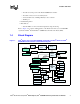
Product Overview — Two RS-232 serial ports from the Intel® 6300ESB I/O Controller — Two PS/2 connectors for mouse and keyboard — On-board VGA Video, ATI Rage Mobility* video controller — Parallel port • Dual Watchdog Timer • Miscellaneous — National LM93* for fan control and temperature/voltage monitoring Refer to Figure 1 for complete detailed features of the Intel® Xeon™ Processor with 800 MHz system bus and Intel® E7520 and Intel® 6300ESB Customer Reference Board (CRB). 1.4 Block Diagram Figure 1.
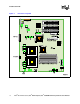
Product Overview Figure 2. Placement - Top View 1& ' 1 &0 PXH $ 2 1& 1 &0 1& 1 &0 '!' '!' %& - . * /$ 1 .. &0 - . * /$ 1 .. &0 *+ ,, + Intel® 6300ESB I/O Controller # *+ ,, + () - .
Product Overview 1.4.1 Memory Subsystem The memory subsystem is designed to support Double Data Rate2(DDR2) Synchronous Dynamic Random Access Memory (SDRAM) using the Intel(R) E7520 MCH. The MCH provides two independent DDR channels, which support DDR2 400 DIMMs. The peak bandwidth of each DDR2 branch channel is 3.2 Gbyte/s (8 bytes x 400 MT/s) with DDR2 400. The two DDR2 channels from the MCH operate in lock step; the effective overall peak bandwidth of the DDR2 memory subsystem is 6.
Product Overview 1.5 Memory Population Rules and Configurations The system supports two DDR2 400 DIMM slots for Channel A and two DDR2 400 DIMM slots for Channel B. The four slots are interleaved and placed in a row in the following order: A1, B1, A2, B2, with A1 being closest to the MCH. This design supports only registered ECC-enabled DIMMs. When populating both channels, always place identical DIMMs in sockets that have the same position on Channel A and Channel B (i.e.
Platform Management Platform Management 2 The following sections describe how the system power management operates and how the different ACPI states are implemented. Platform management involves: • ACPI implementation specific details • System monitoring, control and response to thermal, voltage and intrusion events • BIOS security 2.1 Power Button The system power button is connected to the I/O controller component.
Platform Management 2.3.2 S1 State This state is entered via a processor Sleep signal from the I/O controller (processor C3 state). The system remains fully powered with memory contents intact but the processors enter their lowest power state. The operating system disables bus masters for uniprocessor configurations while flushing and invalidating caches before entering this state in multiprocessor configurations.
Platform Management 2.3.6 S5 State This state is the normal off state whether entered through the Power Button or Soft Off. All power is shut off except for the logic required to restart. The system remains in the S5 State only while the power supply is plugged into the electrical outlet. If the power supply is unplugged, this is considered a Mechanical OFF or G3. 2.3.
Platform Management 2.5.1 Processor Thermal Management Each processor monitors its own core temperature and thermally manages itself when it reaches a certain temperature. The system also uses the internal processor diode to monitor the die temperature. The diode pins are routed to the diode input pins in the LM 93. The LM 93 can be programmed to force the processor fans to full speed operation when it senses the processor core temperature exceeding a specific value.
Equipment Required for CRB Usage Equipment Required for CRB Usage 3 The following components are required for the Intel® Xeon™ Processor with 800 MHz System Bus and Intel® E7520 and Intel® 6300ESB Customer Reference Board (CRB) usage: • A 550 W SSI EPS 12 V power supply. The CRB is shipped with the power supply. • At least two modules of DDR2 400 DIMM. The CRB is shipped with 2 x 256 Mbytes of DDR2 400.
Equipment Required for CRB Usage 3.2 Driver and OS Requirements The required INF driver for the CRB supports the functionality of the Intel® 6300ESB I/O Controller and PXH. The INF file will be included with Red Hat compatible drivers on the CD shipped with the kit. The CRB supports these operating systems: • Microsoft Windows* XP, Windows Embedded XP, 2000 Pro, 2000 Server, 2000 Advanced Server, 2003 Standard Edition • • • • Red Hat Linux Advanced Server 2.1, Red Hat 8.0 on kernel 2.4.
Equipment Required for CRB Usage patches/ide-sata/pci_irq-hr-ich5.patch integrated into the ESB & ICH5 Southbridges patches/lspci/pciids-112202.patch patch to update 2.4.20 pci.ids file patches/lspci/pciids-112202-hr.patch patch to add ESB dev IDs to pci.ids patches/lspci/pciids-112202-hr-ich5.patch patch to add ICH5 dev IDs to pci.ids patches/ioapic/irqbalance-2.4.20-MRC.patch patch for use with P4 Hyper-Threading patches/smbus/i2c-hr.patch enables ESB SMBUS dev in I2C driver patches/smbus/i2c-hr-ich5.
Equipment Required for CRB Usage patches/ide-sata/pci_irq-hr-ich5.patch integrated into the esb6300 & ich5 southbridges patches/lspci/pci.ids-hr.patch adds esb dev ids to 2.4.9-e.24 pci.ids patches/lspci/pci.ids-hr-ich5.patch adds ich5 dev ids to 2.4.9-e.24 pci.ids patches/smbus/i2c-hr.patch enables esb smbus dev in i2c driver patches/smbus/i2c-hr-ich5.patch enables ich5 smbus dev in i2c driver patches/smbus/i2c-2.7.0-Makefile.patch customizations for i2c-2.7.0 Makefile patches/smbus/lm_sensors-2.7.
Jumpers and Headers 4 Jumpers and Headers This section describes the platform component placement as well as configuration, test and debug features of the Intel® Xeon™ Processor with 800 MHz System Bus and Intel® E7520 and Intel® 6300ESB Customer Reference Board. 4.1 Jumpers Figure 4 depicts all jumpers on the CRB. Table 4 illustrates the settings and usage of the jumpers. Review Table 4 and Figure 4 before changing default setting of the jumpers on the CRB. Figure 4.
Jumpers and Headers Table 4. Jumper Settings (Sheet 1 of 3) Jumper Name Ref Des 3.3V Aux Enable J1A1 Enable PXH J2G2 Description/Settings Enables 3.3 V AUX 1-2: Enable 3.3 V AUX for wake events Open: 3.
Jumpers and Headers Table 4.
Jumpers and Headers Table 4. Jumper Settings (Sheet 3 of 3) Jumper Name Ref Des Intel 6300ESB I/O Controller Safe Mode J5F3 CMOS Clear J5H1 Validation Only J5H2 Description/Settings Default Position Intel 6300ESB I/O Controller Safe Mode 1-2: Safe Mode Open: Normal Mode Open Clears CMOS 1-2: Normal 2-3: Configure Validation only Do Not Install Jumper 1-2 Open Access to ICH SMBus Do not Install Jumper ICH SMBUS header J5H3 1: ICH_SMBDAT Open 2. Ground 3.
System Overview 5 System Overview 5.1 Power Diagrams Figure 5 shows the power distribution for the CRB. Refer to the CRB schematics for details on the power distribution logic. (Contact your Intel field sales representative to obtain the schematics file.) Figure 5.
System Overview 5.2 Platform Clocking The CRB uses one CK409B Clock Synthesizer to generate the host differential pair clocks and the 100 MHz differential clock to the DB800. The DB800 then generates the 100 MHz differential pair clock for the PCI Express* devices. Figure 6 shows the CRB clock configuration.
System Overview 5.3 Platform Resets Figure 7 depicts the reset logic for the CRB. The Intel 6300ESB I/O Controller provides most of the reset following assertion of power good and system reset. However, the glue logic within the SIO is also used to buffer reset to PXH, MCH, FWH, and IDE.
System Overview 5.4 SMBus Figure 8 below illustrates the routing of the SMBus signal among the components. Figure 8.
System Overview 5.5 Platform IRQ Routing Figure 9 shows that the Intel 6300ESB I/O Controller uses these segments: • • • • IRQ14 and 15 for IDE segment SERIRQ for SIOPIXRQ segment PCRIRQ for the PCI-X segment PIRQ for the PCI 32/33 segment A Message Signalled Interrupt (MSI) scheme is used between the MCH and PXH over the PCI Express bus. The PXH uses PAIRQ for the Channel A interface to PCI-X 64-bit/100 MHz peripherals and PBIRQ for the Channel B interface to PCI-X 64/133.
System Overview 5.6 VRD VID Headers Provides for manual control of the processor core voltage regulator output level(s). Normally, the processor should be run at its default VID (voltage identification) value as set during manufacturing. However, in the event the user needs to set a different VID value from the default value, it can be accomplished through a jumper block found on the board. Note that these headers are not populated by default. The CPU 0 VID header is located at J9K2.
System Overview Table 5. Processor VRD Settings (Sheet 2 of 2) 0 1 1 1 1 1 OFF 0 0 1 1 1 1 1.4875 1 1 1 1 1 0 1.1000 1 0 1 1 1 0 1.5000 0 1 1 1 1 0 1.1125 0 0 1 1 1 0 1.5125 1 1 1 1 0 1 1.1250 1 0 1 1 0 1 1.5250 0 1 1 1 0 1 1.1375 0 0 1 1 0 1 1.5375 1 1 1 1 0 0 1.1500 1 0 1 1 0 0 1.5500 0 1 1 1 0 0 1.1625 0 0 1 1 0 0 1.5625 1 1 1 0 1 1 1.1750 1 0 1 0 1 1 1.5750 0 1 1 0 1 1 1.
System Overview 5.7 Miscellaneous Buttons Figure 10 below shows the location of the power buttons within the platform. Figure 10.
Debug Procedure 6 Debug Procedure The debug procedures in this section are used to determine baseline functionality for the Intel® Xeon™ Processor with 800 MHz System Bus, Intel® E7520 Chipset, and Intel® 6300ESB ICH Development Kit. This is a cursory set of tests designed to provide a level of confidence in the platform operation. 6.1 Level 1 Debug (Port 80/BIOS) Refer to the steps in Table 6 when debugging a board that does not boot. Table 6.
Debug Procedure 6.2 Level 2 Debug (Power Sequence) Check the items in Table 7 below if “SYSTEM PWRGD” is not illuminated. Table 7. Level 2 Debug (Power Sequence) Item Test Pass/Fail Criteria Cause of Failure Measure voltage across: • C3K2: 3.3 V 1 Primary power supply voltages • C3K1: -12 V • C4K3: 5 V External power supply failure • C4K2: 5 V • C4K5: 12 V 2 1.8 V C9E14: 1.8 V DDR2 power supply failure 3 1.5 V C5C5: 1.5 V MCH/PXH/ICH core power supply failure 4 1.8 VSBY C9G5: 1.
Heatsink Assembly 7 Heatsink Assembly This section provides heatsink assembly instructions for the Intel® Xeon™ Processor with 800 MHz System Bus, Intel® E7520 Chipset, and Intel® 6300ESB ICH Development Kit: Components requiring post-secondary heat sink assembly are listed in Table 9. Table 9. Components Requiring Heat Sink Assembly Component Processors (See Figure 11.) Figure 11.
Heatsink Assembly 7.1 Processor Heat Sink Installation Instructions Note: Tools/items needed include Phillips screwdriver, disposable towels, and isopropyl alcohol. 1. Ensure the processor is firmly seated in the socket and the socket latch is closed. (See Figure 12.) Figure 12. Inserting Processor in Socket 2. Clean the processor’s top surface with a clean towel and isopropyl alcohol. (See Figure 13.) Figure 13.
Heatsink Assembly 3. Insert the processor heat sink back plate into the four mounting holes near the processor. The back plate is assembled to the back side of the PCB. (See Figure 14.) Figure 14. Installing the Processor Backplate 4. Remove the protective covers from the processor heat sink. There is a cover that protects the fan, and another that protects the preapplied thermal interface material on the bottom of the heat sink base. (See Figure 15.) Figure 15.
Heatsink Assembly Figure 16. Installing the Heatsink Tighten screw 1 Tighten screw 4 Tighten screw 3 Tighten screw 2 6. Using a Phillips screwdriver, tighten the screws in the pattern indicated in Figure 16. The screws are shoulder screws and will stop threading once completely tightened. 7. Plug the fan connector into the nearest fan connector on the PCB. 8. If applicable, repeat this process for the second processor.