
ITP700 Debug Port Design Guide

R
ITP700 Debug Port Design Guide 27
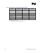
Debug Port Signal Layout Guideline
FBI FBI is a fast edge copy of TCK that can optionally be used as the source of
scan chain TCK when TCK buffers are implemented on a system board. FBI
should be loaded with no greater than 40 pF and have a DC load of no less
than 200 Ω to GND. If used, this is a critical clock for the scan chain and must
be analyzed for signal quality and timing with respect to the specifications of the
intended receiver of the FBI signal.
DBR# This is a non-critical route.
DBA# This is a non-critical route.
NOTE: Refer to BCLK system requirements for proper termination requirements and routing rules.
DBA# and DBR# are output signals from the ITP. The ITP provides an open drain FET closure to
GND as the drive of DBA# and DBR#. The target system should provide the pull-up for both of
these signals. The pull-up can be to any voltage up to five volts that is consistent with the input
specifications of the component used to receive these signals on the target system. DBR# is the
ITP debug port reset signal that should always be routed to the system reset controller. DBA# is
the ITP debug port scan active signal used to indicate that the ITP is currently driving the scan
chain. DBA# is an optional signal of the debug port.
2.3.2 JTAG Signal Layout Guidelines
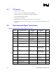
Table 12. JTAG Signal Layout Guidelines
Debug Port Signal Layout Guideline
TCK This is a critical JTAG clock signal, sourced by the debug port, which requires
thorough timing and signal integrity analysis/simulation. Since there are usually
multiple loads on TCK, a matched star topology of up to 8 arms, and
originating within 200 ps of the debug port is strongly recommended. The
termination resistor to GND on TCK must be located within 200 ps of the
debug port in order to minimize IR losses that would degrade signal voltage
levels at the loads. Arms for the TCK star should not exceed 2 ns in electrical
length and all arms should be matched within 100 ps. Note that one arm of the
star should return a feedback copy of TCK to FBO at the debug port. The
length of the trace between the processor or chipset TCK pin on this arm and
the debug port must be equal to the electrical length of BPM[5:0] and RESET#
from the closest system bus agent to the debug port. Load capacitance at the
end of each arm must be no more than 35 pF. It is strongly recommended that
this signal be simulated for signal integrity purposes. Non-monotonicity on the
rising or falling edge of TCK will render the ITP inoperative. See the Execution
Signal Layout Guidelines section of this chapter for additional information.
TMS Critical JTAG mode select signal, sourced by the debug port, which requires
moderate timing and signal integrity analysis / simulation. Since there are
usually multiple loads on TMS, a matched star topology of up to 8 arms, and
originating within 200 ps of the debug port is recommended. The termination
resistor to VTAP on TMS should be located within 200 ps of the debug port in
order to minimize resistive losses that would degrade signal voltage levels at
the loads. Arms for the TMS star should be matched within 400 ps to the
length of the TCK star.