
Intel Xeon Processor and Intel E7500/E7501Chipset Compatible Platform Design Guide

Intel
®
Xeon™ Processor and Intel
®
E7500/E7501 Chipset Compatible Platform Design Guide 177
Platform Power Delivery Guidelines
Processor VCC_CPU static and transient tolerances and the corresponding Voltage Regulator
tolerances assume power distribution paths with resistances no greater than 0.4 m
Ω and
inductances no greater than 0.1 nH. Meeting these limits can be a challenge because of system
layout constraints.
Refer to Figure 3-1 for the recommended stack-up showing power and ground layer
implementation. Power must be distributed as a plane. This plane can be constructed as an island
on a layer used for other signals, on a supply plane with other power islands, or as a dedicated layer
of the PCB. Processor power should never be distributed by traces alone.
Because processor voltage is unique to most system designs, a voltage island is probably the most
cost-effective means of distributing power to the processors. This island should not have any
breaks from the source of power to the load to minimize inductance in the plane. It should
completely surround all of the pins of the source and all of the pins of the load.
Use a 2 oz. copper power plane for VCC_CPU and a 2 oz. copper power plane for ground. Using
the recommended power and ground plane copper weight and geometries minimizes resistance and
inductance in the planes that affects the ability of the voltage regulator and decoupling to meet the
DC and AC power requirements of the processors. This can be implemented on two 1 oz. copper
layers or four 1/2 oz. copper layers. The bulk capacitors can be placed close to the processors, and
the high-frequency capacitors should be placed next to the processors. Distribute the bulk and high-
frequency capacitors equally on both sides of the socket where the power/ground pins are located.
The Intel Xeon processor socket has 603 or 604 pins (depending on processor package: refer to
Table 1-4) with a 50-mil pitch. The routing of the signals, power, and ground pins require creation
of may vias. These vias cause a “swiss cheese” effect in the power and ground planes beneath the
processor, resulting in increased inductance of these planes. To minimize this swiss cheese effect,
the power / ground planes should completely surround all of the pins of the VRM or VRD and
processor socket. Also minimize the size of the processor socket vias’ anti-pads where possible.
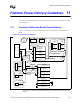
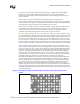
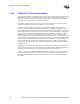
Anti-pads should be no larger than 35 mils. Figure 11-2 shows an example of good socket power/
ground plane routing for an inner layer. Note the absence of plane cuts or other plane
discontinuities that inhibit the current flow to these power pins. Bad power/ground routing to the
processor socket pin vias and large anti-pads reduce the amount of effective copper, which may
result in highly inductive current paths in the socket breakout region. Locations of the capacitor
pads on the outer power layer should not hinder power distribution by creating a “slot”-shaped
geometry in the plane. This can limit the ability of the decoupling capacitors and/or voltage
regulator to supply the necessary current response to processor transients. It is recommended that
you place as many high-frequency capacitors as possible inside the cutout of the processor socket.
The remaining high-frequency capacitors should be placed next to the processor, specifically near
the power/ground pins.
Figure 11-2. Example of Good Plane Distribution to Power or Grounds of the Processor
Socket