
ITP700 Debug Port Design Guide


R
38 ITP700 Debug Port Design Guide
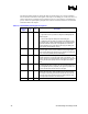
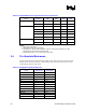
Table 19. ITP700 DPA Execution Signal DC Electrical Characteristics
Signal Min Max Unit Note
I
OL
120 mA 1
R
OL
18 Ω 2
BPM5DR#
C
IN
4 pF 3
V
IH
PWR + (0.15*VTERM) 3.00 V 4
V
IL
PWR -
(0.15*VTERM)
V 4
I
IH
-150 uA
I
IL
300 uA
BPM[5:0]#,
RESET#
C
IN
3 pF 3
NOTES:
1. Maximum sink current of the ITP.
2. Series resistance to GND when output is low.
3. Includes capacitive effects of mated connector.
4. Over valid range of VIH of PWR.
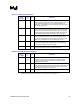
3.3 ITP700 DPA AC Electrical Characteristics
Table 20. ITP700 DPA System Signal AC Electrical Characteristics
Signal Parameter Min Max Unit Note
PWR PWR V
IL
Max to Tristate 150 µs
Rise Time 0.5 2 ns 1, 2, 3
Fall Time 0.5 2 ns 1, 2, 3
FBI
Skew -9 -6 ns 4
DBA#↓ to first TCK↑ 75 ns 5 DBA#
DBA#↑ to last TCK↓ 100 ns 6
DBR# DBR# Assertion Period 150 µs
NOTES:
1. Measured from 20% to 80% of transition.
2. Measured into a load to GND of 220 Ω and 10 pF.
3. FBI has the same period; time High, and time Low specifications as TCK.
4. With respect to same edge on TCK.
5. Measured from assertion of DBA# to 50% of first TCK transition.
6. Measured from release of DBA# to 50% of last TCK transition.