
Intel Xeon Processor and Intel E7500/E7501Chipset Compatible Platform Design Guide

Platform Clock Routing Guidelines
58 Intel
®
Xeon™ Processor and Intel
®
E7500/E7501 Chipset Compatible Platform Design Guide
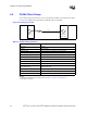
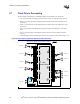
4.5 CLK14 Clock Group
The driver in the CLK14 clock group is the clock synthesizer 14.318 MHz clock output buffer
(pin REF0), and the receiver is the 14.318 MHz clock input buffer at the ICH3-S, SIO, and LPC.
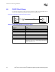
Figure 4-13. Topology for CLK14
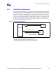
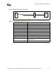
Table 4-8. CLK14 Routing Guidelines
Parameter Routing Guidelines
Clock Group CLK14
Topology Point-to-Point
Reference Plane Ground referenced (contiguous over entire length)
Characteristic Trace Impedance (Z
0
) 50 Ω ± 10%
Trace Width 5 mils
Trace Spacing 10 mils
Trace Length – L1 0.00” – 0.50”
Trace Length – L2 3.00” – 9.0”
Resistor R1 = 22
Ω ± 5%
Skew Requirements None
R1
L1
L2
Intel
®
ICH3-S
SIO, and LPC
REF0
CK408