
ITP700 Debug Port Design Guide


R
ITP700 Debug Port Design Guide 49
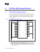
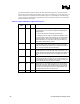
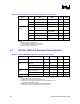
Table 28. ITP700 LVDPA JTAG Signal DC Electrical Characteristics
Signal Min Typ Max Unit Note
V
OH
0.9*VTAP VTAP + 0.250 V 2
V
OL
0 0.1*VTAP V 2
I
OH
-60mA mA
I
OL
0 mA
TCK
Z
TCK
20 Ω 3
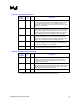
V
OH
0.9*VTAP VTAP + 0.250 V 4
V
OL
0 0.1*VTAP V 4
I
OH
-16 mA
I
OL
36 mA
TMS
Z
TMS
20 Ω 3
V
OH
V 5
V
OL
0 0.1*VTAP V 1
I
OH
0 mA
TDI
I
OL
8 mA
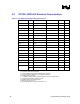
V
OH
0.9*VTAP VTAP + 0.250 V 1
V
OL
0 0.1*VTAP V 1
I
OH
-8 mA
TRST#
I
OL
8 mA
V
IH
0.5*VTAP +0.150 V
V
IL
0.5*VTAP -0.150 V
I
IH
-100 µA
TDO
I
IL
100 µA
NOTES:
1. At maximum current specified.
2. As measured into a 27 Ω 1% resistor to GND.
3. AC Impedance of the driver.
4. As measured into a 39 Ω 1% resistor to 1.10V.
5. Open Drain Driver on the LVDPA