
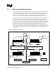
ITP700 Debug Port Design Guide


R
ITP700 Debug Port Design Guide 45
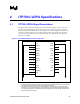
4 ITP700 LVDPA Specifications
4.1 ITP700 LVDPA Signal Descriptions
The signals used by the ITP700 LVDPA are divided into three categories: system, JTAG, and
execution. The system signal group indicates the access state of the entire system. The JTAG
signal group indicates the IEEE 1149.1 control signals. The execution signal group contains the
reset and run control signals used to coordinate debug activities. The signals in the execution
group are system bus signals and are recovered on BCLK. The signals in the JTAG group can
operate up to 16 MHz.
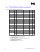
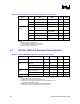
Figure 13. ITP LVPDA Debug Port Pinout (Top View)
1 GND
3 BPM[0]#
5 BPM[1]#
7 BPM[2]#
9 BPM[3]#
11 BPM[4]#
13 BPM[5]#
15 RESET#
17 FBO
19 BCLKp
21 BCLKn
23 BPM5DR#
25 GND
DBA# 4
DBR# 6
GND 8
TDI 10
TMS 12
TRST# 14
TCK 16
FBI 18
GND 20
PWR 22
TDO 24
GND 2
NOTES:
1. All execution signals, BCLK(p/n), and all JTAG signals must be simulated and routed with care. See the
appropriate generic layout and processor specific chapters for details.
2. The system clock of the processor may reference BCLK[1:0] where BCLK0 is the rising edge for the
beginning of any transaction and BCLK1 as the falling edge. The ITP uses BCLK[p/n] where BCLKp is
the rising edge and BCLKn is the falling edge for the beginning of any transaction. All routing Rules for
the BCLK signals do not change.