
Intel Xeon Processor Multiprocessor Platform Design Guide


43
System Bus Routing
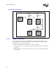
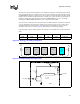
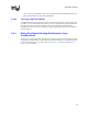
Using the recommendations for via size shown in Figure 6-8 will ensure that two traces can be
routed between vias and that the traces are overlapping the reference planes by at least 50%. The
overlap should occur only for a short distance. The use of 4.0 mil wide traces allows good trace
spacing to be maintained through the socket pin field. Three-dimensional simulation is
recommended for determining the impact of signals without a solid reference plane.
6.4.2 Routing Guidelines for Asynchronous GTL+ and Other
Signals
This section describes layout recommendations for signals not covered in the previous section.
Table 6-4 shows the signals covered in this section. Each topology will be described in detail in the
following sections. All signals must meet the AC and DC specifications listed in the processor
datasheet.
Figure 6-8. 0.025" Via Pad with 50% of Trace over Reference Plane
15 mil power plane
30 mil routing path
2.5 mils2.5 mils
5 mils5 mils
15 mil power plane
15 mil power plane
4 mil Signal Trace
4 mil Signal
Trace
Assumptions :
Inner signal layers:
10 mil via hole
5 mil clearance
Inner plane layers:
35 mil antipad
Outer plane layers:
25 mil surface anti-pad
Top View
Cross-sectional
View
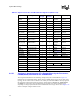
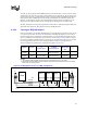
Table 6-4. Asynchronous GTL+ and Miscellaneous Signal List (Sheet 1 of 2)
Signal Name Type
Processor
I/O Type
Topology
Number
Driven by Received by
A20M# Asynchronous GTL+ I 2 Chipset Processor
BR[3:1]# AGTL+ I 5 Processor Processor
BR0# AGTL+ I/O 5 Processor
Processor/
Chipset
BINIT# AGTL+ I/O 13
Processor/
Chipset
Processor
COMP[1:0] Other I 6 Pull-Down Processor
FERR# Asynchronous GTL+ O 1 Processor Chipset
IERR# Asynchronous GTL+ O 1 Processor
IGNNE# Asynchronous GTL+ I 2 Chipset Processor
INIT# Asynchronous GTL+ I 2 Chipset Processor
LINT[1:0] Asynchronous GTL+ I 2 Chipset Processor