
Intel Xeon Processor Multiprocessor Platform Design Guide

70
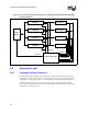
Processor Power Distribution Guidelines
Where N is the number of V
CC
/V
SS
planes. To minimize parasitic layer inductance, it is important
to reduce the distance from decoupling capacitors to the processor socket (reducing
l) and to use
islands for power distribution (increasing
w). To reduce h, it is recommended to select the V
CC
/V
SS
planes in the layer stack up that are interleaved and have small spacing in between. As a practical
matter it is impossible to get the requisite baseboard inductance without locally dedicating at least
4 planes to carry power from the baseboard capacitors to the power pins of the processor.
There are impedance consequences for signals that cross over or under the edges of the Power
Island that exists on another layer. While neither of these may be necessary for most designs, there
are two reasonable options to consider which can protect a system from these consequences.
Processor power islands can be isolated from signals by one of the solid power plane layers such as
the ground layer. This forces a particular stack-up model.
Another option that helps, but does not completely eliminate radiation effects, is to decouple the
edges of the processor power islands to ground on regular intervals of about 1 inch, using good
high-frequency decoupling capacitors (1206 packages). This requires more components but does
not require any particular board stack-up.
In either case, for controlling emissions, all planes and islands should be well decoupled. The exact
board layout, and the chassis design will determine the amount of decoupling required for
controlling emissions. One should plan ahead by allowing additional pads for capacitors to be
added in case they are found to be necessary during EMI testing.
Signals routed over power islands or islands in the ground plane create a discontinuity in the return
path of that signal. This discontinuity can have detrimental effects on the timing and signal quality
of that signal and other signals referencing the same planes. Avoid routing signals over splits in
power planes or ground planes at all times.
Example:
Given power bussing area from the regulator to the socket approximated as a rectangle, with the
following dimensions for the power and ground plane:
l = 0.279 inch; w = 2.09 inches; t =
1.24 mils (1 oz. copper):
The total resistance of the round trip is:
With the V
CC
-V
SS
separated by 4.5 mils, the loop inductance is:
Ω=
⋅
⋅⋅Ω= m 073.0
lm24.1.092
"279.0
milm 677.0
i
R
Ω=Ω⋅= m 15.0m 073.02R
pH 2.19
1)-(2mil 09.2
mil 5.4mil 279.0
mil
pH
9.31 =
⋅
⋅
⋅=L