
Intel Xeon Processor Multiprocessor Platform Design Guide


18
System Overview
processor family system bus, but is not compatible with the P6 processor family system bus. The
system bus uses Source-Synchronous Transfer (SST) of address and data to improve performance.
Whereas the P6 processor family data transfer is once per bus clock, the Intel Xeon processor MP
and Intel Xeon processor MP with up to 2-MB L3 cache on the 0.13 micron process transfer data
four times per bus clock (4X data transfer rate, as in AGP 4X). Along with the 4X data bus, the
address bus can deliver addresses two times per bus clock and is referred to as a “double-clocked”
or 2X address bus. In addition, the Request Phase completes in one clock cycle. Working together,
the 4X data bus and 2X address bus provide a data bus bandwidth of up to 3.2 GB per second.
Finally, the system bus also introduces transactions that are used to deliver interrupts.
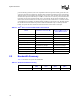
2.2 Bandwidth Summary
Table 2-2 documents the system bus bandwidth.
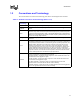
Table 2-1. Intel
®
Xeon™ Processor MP Feature Set Overview
Feature Intel
®
Xeon™ Processor MP
Intel
®
Xeon™ Processor MP
with up to 2-MB L3 Cache on
the 0.13 Micron Process
L1 Cache On-die On-die
L2 Cache 256 KB on-die 512-KB on-die
L3 Cache 512 KB or 1 MB on-die 1-MB or 2-MB on-die
Data Bus Frequency 400 MHz 400 MHz
Multi-processor Support 1-4 way 1-4 way
Manageability Features
PIROM, Scratch EEPROM, and
thermal sensor on package
PIROM, Scratch EEPROM, and
thermal sensor on package
Processor Core Voltage 1.7 V 1.5 V
Processor Socket 603-pin 603-pin
Processor Package 603-pin micro-PGA 603-pin micro-PGA
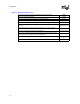
Table 2-2. Platform Bandwidth Summary
Interface
Clock Speed
(MHz)
Samples per
Clock
Data Width
(Bytes)
Bandwidth
(MB/s)
System bus (4-way) 100 4 8 3200