
Intel Xeon Processor and Intel E7500/E7501Chipset Compatible Platform Design Guide


High-Speed Design Concerns
220 Intel
®
Xeon™ Processor and Intel
®
E7500/E7501 Chipset Compatible Platform Design Guide
buffers, balancing setup and hold time requirements of the receiver, and other electrical factors
verified in simulation and system bus validation. For the system bus recommendations included in
this document, Equation 12-4 is used:
Equation 12-4. Signal Integrity Adjustment Length
Signal X
SI Adj
= 0.78 * SignalX
PLC
The 0.78 compensation factor was determined to be the optimum adjustment for the system bus
recommendations given in this platform design guide.
12.6.3 Final Length Matching Equation
This section explains the final length matching compensation scheme, associated equations, and an
explanation for determining the motherboard trace lengths. Processor Length Matching is only
dependant upon a signals PLC and the SI motherboard. To determine an actual PCB length, the
designer can use one signal as a reference signal to calculate the PCB length of the remaining
signals in a group. For simple illustrative purposes, the formulas and examples used are based upon
the shortest PCB trace length. However, the formulas could be based off any signal in the group.
For simple illustrative purposes, the example also assumes the shortest and longest signals on the
processor package are the shortest and longest for the MCH package as well. This is not necessarily
the case.
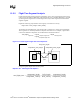
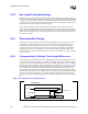
Figure 12-15 contains the final length matching example that accounts for PLC and SI Adjustment
Length compensation in the motherboard trace lengths. The signal whose motherboard trace length
between Processor 0 and Processor 1 has the longest Processor package length has no Signal
Adjustment Length Compensation (denoted as “SI”) in the Processor 0/Processor 1 path. All
source synchronous signals with less than the longest processor and MCH package length require
varying amounts of PLC and SI motherboard length segments added to
Shortest Signal
Processor 0
to Processor 1 PCB Length
and Shortest Signal
Processor 1 to MCH PCB Length
respectively. The example
in Figure 12-15 shows SI adjustment for the strobe signal, but the strobe signal could be replaced
with any data signal with a processor package length that is not the maximum in that group.
It is important to note that PLC is only performed for the components at the endpoints of the
system bus (i.e., Processor 0 and the MCH). At the components in the middle of the bus, the SI
factors is used. Since SI is a scaling factor of the PLC, the PLC is still taken into consideration at
the middle of the bus. Additional PLC segments on both sides of Processor 1 would certainly
balance the total pad-to-pad length for the Processor 0/Processor 1 and Processor 1/MCH paths.
Figure 12-15. Final Illustration of PLC and SI Length Matching
Longest Package
Trace Length
Shortest Package
Trace Length
Di e
Pa d
Component Pin
Shortest Signal
Processor 1 to Processor
0 PCB Length
Processor 0
0.78 *
Pr oc PL C
Die
Pa d
MC H PL C
MCH
Pr oc PLC
Del ta Pr oc
Delta Pr oc Delta MCH
Del ta MCH
Processor 1
Zero for longest
package trace signal
Die Pad
Shortest Signal
Processor 1 to Processor
0 PCB Length
Shortest Signal
Processor 1 to MCH
PCB Length
Shortest Signal
Processor 1 to MCH
PCB Length
0.78 *
Pr oc PL C
Shortest Package
Trace Length
0.78 *
Pr oc PL C
0.78 *
Pr oc PL C
Longest Package
Trace Length
Shortest Package
Trace Length
Longest Package
Trace Length