
Intel Xeon Processor and Intel E7500/E7501Chipset Compatible Platform Design Guide

Intel
®
Xeon™ Processor and Intel
®
E7500/E7501 Chipset Compatible Platform Design Guide 59
Platform Clock Routing Guidelines
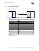
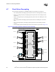
4.6 USBCLK Clock Group
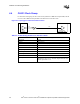
For the USBCLK clock group, the driver is the clock synthesizer USB clock output buffer
(pin USB-48MHz), and the receiver is the USB clock input buffer at the ICH3-S (pin CLK48).
Note that this clock is asynchronous to any other clock on the board.
Figure 4-14. Topology for USB_CLK
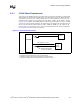
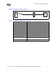
Table 4-9. USBCLK Routing Guidelines
Parameter Routing Guideline
Clock Group USBCLK
Topology Point-to-Point
Reference Plane Ground referenced (contiguous over entire length)
Characteristic Trace Impedance (Z
0
) 50 Ω ± 10%
Trace Width 5 mils
Trace Spacing 25 mils
Trace Length – L1 0.00” – 0.50”
Trace Length – L2 3.00” – 12.00”
Resistor R1 = 33
Ω ± 5%
Skew Requirements None – USBCLK is asynchronous to any other clock on the board
Maximum Via Count 2
R1
L1
L2
Intel
®
ICH3-S
CK408
USB-
48 MHz
CLK48