
Intel Xeon Processor Multiprocessor Platform Design Guide

74
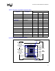
Processor Power Distribution Guidelines
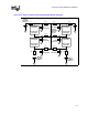
inductance and resistance of the power plane between voltage regulator and bulk capacitors and the
processor is shown as L1 and L7. A current step from 0 A to 55 A should be applied with a rise
time of 308 ns or use the PWL values.
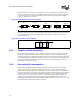
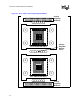
Figure 8-5. Processor Lump Model Schematic
North Side
Socket Power
Pin Field
1206s north
Lskt
L1 L2 L6 L7
1206s south
1206s int
Lint
DIP
Lcore
Core
Lcore
DIP
Lint
Lskt
1206s int
L3 L4 L5
1206s north
cavity
1206s south
cavity
South Side
Socket Power
Pin Field
North Side
Input
South Side
Input