
Intel Xeon Processor and Intel E7500/E7501Chipset Compatible Platform Design Guide

Intel
®
Xeon™ Processor and Intel
®
E7500/E7501 Chipset Compatible Platform Design Guide 91
Memory Interface Routing Guidelines
6.4 Source Clocked Signal Group Routing
The MCH drives the command clock signals and the source-clocked signals together. That is, the
MCH drives the command clock in the center of the valid window, and the source-clocked signals
propagate with the command clock signal. Therefore, the critical timing is the difference between
the command clock flight time and the source clocked signal flight time. The absolute flight time is
not as critical.
If you use resistor packs for the termination resistors, it is suggested that data group signals not be
mixed with Source Clocked, Chip Select, or Clock Enable signals within the same resistor pack for
validation purposes.
f
NOTES:
1. On a compatible motherboard, use a 33.2 Ω for an E7500 chipset MCH and a 39.2 Ω for an E7501 chipset
MCH.
NOTES:
1. Indicated lengths measure from the MCH component pin to the DIMM connector pin.
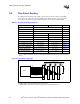
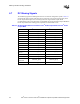
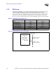
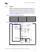
Table 6-6. Source Clocked Signal Group Routing Guidelines
Parameter 3-DIMM Solution 4-DIMM Solution Reference
Signal Group RAS#, CAS#, WE#, MA[12:0], BA[1:0]
Topology Daisy Chain Figure 6-9
Reference Plane Ground Figure 6-5
Trace Impedance (Z
0
) 50 Ω ± 10% 50 Ω ± 10% Table 6-2
Nominal Trace Width 5 mil 5 mil Figure 6-5
Nominal Trace Spacing 15 mil 15 mil Figure 6-5
MCH to DIMM1 Trace Length 2.0” to 6.0” 2.0” to 6.0” Figure 6-9
DIMM to DIMM Trace Length 1.0” to 1.2” 1.0” to 1.2” Figure 6-9
DIMM to Rtt Trace Length < 0.8” 0.3” to 1.3” Figure 6-9
Termination Resistor (Rtt) 39.2
Ω ± 1% / 33.2 Ω ± 1%
1
34.8 Ω ± 1% Figure 6-9
MCH Breakout Guidelines 5/5, < 500 mil 5/5, < 500 mil
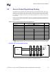
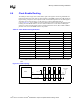
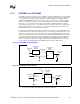
Figure 6-9. Source Clocked Signal Topology
DIMMs
MCH
RAS#, CAS#, WE#
MA[12:0], BA[1:0]
DDR VTERM
(1.25 V)
MCH to DIMM1
DIMM to
DIMM
Rtt
Rtt
DIMM to
DIMM
DIMM to
DIMM
DIMM
to Rtt