
Voltage Regulator Module (VRM) 10.2L Design Guidelines

Output Voltage Requirements
12 Voltage Regulator Module (VRM) 10.2L Design Guidelines
2.4 Stability - REQUIRED
The VRM needs to be unconditionally stable under all specified output voltage ranges, current
transients of any duty cycle, and up to repetition rates of 1 MHz. The VRM should be stable under
a no load condition.
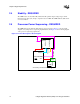
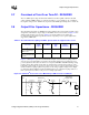
2.5 Processor Power Sequencing - REQUIRED
The VRM must support platforms with defined power-up sequences. Figure 2-3 shows a block
diagram of a system power-on sequencing implementation, and Figure 2-4 shows a timing diagram
of the power-on sequencing requirements.
Figure 2-3. Power-On Sequence Block Diagram
CPU
VCC
VID[5:0]
Vcc VRM/EVRD
Vtt VR
Vcc
VID[5:0]
Vcc_PWRGD
OUTEN
VTT
VTT
VID_PWRGOOD
VIDPWRGD
To System
PWRGD
Delay *
* This Delay could be built into the V
TT
VR