
Intel Xeon Processor and Intel E7500/E7501Chipset Compatible Platform Design Guide

Intel
®
Xeon™ Processor and Intel
®
E7500/E7501 Chipset Compatible Platform Design Guide 227
Schematic Checklist
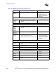
SM_ALERT#
SM_CLK
SM_DAT
• Connect to both processors and SMBus.
• A pull-up resistor to 3.3 V. Resistor value is
based on the number of devices on the
SMBus.
• These signals have 10 k
Ω pull-
downs on the Intel
®
Xeon™
processor with 512-KB L2 cache
and are not supported on the
Intel
®
Xeon™ processor with
533 MHz system bus
• Refer to Section 5.5 and
Section 9.5.4.
SM_EP_A[2:0] • Leave as no connect to set bit low, or pull-up
to 3.3 V through 100
Ω ± 5% resistor to set bit
high.
• Use these address bits to set a unique
SMBus address for the memory devices on
the processor.
• SMBus Input.
• These signals have 10 k
Ω pull-
downs on the Intel Xeon
processor with 512-KB L2 cache
and are not supported on the Intel
Xeon processor with 533 MHz
system bus.
• Refer to Section 5.5 and the
Intel
®
Xeon™ Processor with 512-KB L2
Cache at 1.80 GHz to 2.80 GHz
Datasheet
for more details.
SM_TS_A[1:0] • Use these address bits to set a unique
SMBus address for the thermal devices on
the processor.
• Leave as no connect to set bit to high-
impedance state.
• Pull-up to 3.3 V through 1 k
Ω ± 5% to set bit
high.
• Pull-down to ground through 1 k
Ω ± 5% to
set bit low.
• SMBus Input.
• These signals are not supported
on the Intel Xeon processor with
533 MHz system bus.
• Refer to Section 5.5 and the
Intel
®
Xeon™ Processor with 512-KB L2
Cache at 1.80 GHz to 2.80 GHz
Datasheet
for more details
SM_VCC /
VID_VCC
• Connect to 3.3 V power supply.
SM_WP • 100
Ω ± 5% pull-up to 3.3 V to write-protect
the processor’s Scratch EEPROM.
• Leave as no connect (NC) to disable write-
protecting of Scratch EEPROM.
• SMBus Input.
• Refer to Section 5.5.
TESTHI[6:0] • Option 1: Recommend separate 50
Ω ± 20%
pull-up to VCC_CPU.
• Option 2: TESTHI[3:0] and TESTHI[6:5] may
all be tied together and pulled up to
VCC_CPU with a single 50
Ω resistor if
desired. However, boundary scan test
cannot be performed if these pins are
connected together. TESTHI4 must always
be pulled up independently from the other
TESTHI pins.
• Input.
• Refer to Section 5.3.5.
THERMDA
THERMDC
• Connect to the Cathode and Anode pins of
the thermal sensor.
• Refer to Section 5.5.2.
VCCA • Use discrete RLC filter to provide clean
power.
• An isolated power for internal
PLL.
• Refer to Section 11.2.7.
VCCIOPLL • Use discrete RLC filter to provide clean
power.
• An isolated power for internal
PLL.
• Refer to Section 11.2.7.
Table 13-1. Processor Schematic Checklist (Sheet 3 of 4)
Checklist Items Recommendations Comments