
Intel Xeon Processor and Intel E7500/E7501Chipset Compatible Platform Design Guide

Intel
®
Xeon™ Processor and Intel
®
E7500/E7501 Chipset Compatible Platform Design Guide 185
Platform Power Delivery Guidelines
11.2.5.3 VRD Circuit Implementation
This section contains general VRD circuit and layout implementation recommendations. For
specific VRD design details, refer to the Dual Intel
®
Xeon™ Processor Voltage Regulator Down
(VRD) Design Guidelines and VRD vendor documentation.
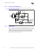
Route the VRD’s voltage sense input signal to the middle of the VCC_CPU plane. The location of
this plane connection and route is not critical. The voltage regulator Pulse Width Modulation
(PWM) uses the voltage sense pin to monitor the VRD output voltage, which is used to generate
the VRD power good signal.
The VRD circuit should contain low-pass filters (RC) on the output of each MOSFET phase. This
filter reduces output noise and helps stabilize the VRD’s operation. The exact filter values will
depend on the voltage regulator PWM controller and MOSFET components used. Include series
inductors at the output of each MOSFET phase. The exact value should be carefully chosen and
will depend on the actual VR components used. Lowering the inductance value increases the
transient current (dI/dt) capability of each output phase, but will increase power dissipation from
the MOSFETs.
Carefully select the switching frequency of the PWM controller using the methods specified by the
PWM vendor. The switching frequency should be chosen to support the static and transient
requirements of both processors. Increasing the frequency will increase the response of the VRD,
but will also increase the power dissipation of the phase drivers and MOSFETs.
Route the positive (and negative if the VRD provides differential inputs) voltage feedback inputs
for the VRD to the VCC_CPU plane with the following conditions.
• They must be connected to the power plane through a series resistor. This resistor should be
sized to provide the correct droop to satisfy the load line requirement.
• They must affect less than 1 Ω roundtrip resistance to minimize the voltage drop between the
sense point and VR input.
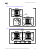
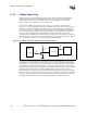
• Route the positive feedback line to a point on the VCC_CPU power plane in the middle of and
equidistant from both processors. Middle is defined as a point that provides the shortest
geometrical mid-point between the centers of the processor sockets.
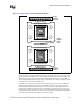
• Route the negative feedback line to the corresponding X-Y location, but on the VCC_VSS
ground plane. See Figure 11-7 and Figure 11-8 for an example of sense point locations for the
example VR topologies.
• Route each of the feedback lines with less than 5 inches total trace length. Do not route near
signal lines unless shielding is provided.
• The trace(s) should be carefully routed to avoid picking up noise.