
Intel Xeon Processor and Intel E7500/E7501Chipset Compatible Platform Design Guide

Intel
®
82870P2 (P64H2)
120 Intel
®
Xeon™ Processor and Intel
®
E7500/E7501 Chipset Compatible Platform Design Guide
8.1.6 Clock Configuration
All PCI clocks must be disabled in the BIOS for any unused/unpopulated PCI/PCI-X slots. The
PxPCLKO[5:0] pins can each be disabled by writing to the Disable PCLKOUT 5 – 0 bits
(DPCLK, bits 15:10, configuration register offset 40h in each bridge). These clocks function the
same in serial and dual-slot parallel modes. In serial mode, the PxPCLKO[5:0] signals are all
driven low when the clock to the slot is disabled by the Hot-Plug controller, regardless of the
DPCLK bits. Once the Hot-Plug controller connects the clock to the slot, these clocks are enabled
again—which clocks are enabled does depend on DPCLK at this point. It is expected that
PxPCLK0 will be connected to the PCI slot in single-slot parallel mode.
NOTES:
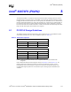
1. The clock signal and feedback loops are closely related. L2 and L
fbi
can be any length, but need to be tuned
to each other ± 25 mils. Refer to Figure 8-9 for L2, and Figure 8-10 for L
fbi
.
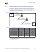
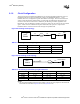
Figure 8-8. Hot-Plug Clock Topology
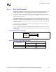
Table 8-11. Hot-Plug Clock Routing Length Parameters
Clock Speed L1 (inches) L2 (inches) L3 (inches)
66 MHz 0.25 – 1.0 (L
fbi
– L3) – 2.523 0.75 – 1.25
100 MHz 3.5 – 4.5 0.25 – 0.5 = L3 0.25 – 0.5 = L2
133 MHz 1.5 – 2.5 0.5 – 1.0 = L3 0.5 – 1.0 = L2
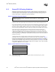
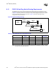
Figure 8-9. No Hot-Plug Clock Topology
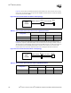
Table 8-12. No Hot-Plug Clock Routing Length Parameters
Clock Speed L1 (inches) L2 (inches) Slot L2 (inches) Device Down
33 MHz Slot 3.5 – 5.5 0.5 – 5.0 2.9 – 7.9
66 MHz 3.5 – 4.5 0.5 – 1.0 3.0 – 3.5
100 MHz
≤ 1.0 L
fbi
– 2.5
1
L
fbi
1
133 MHz ≤ 1.0 L
fbi
– 2.5
1
L
fbi
1
Slot
Intel
®
P64H2
Switch
33 Ω
L3
L1
L2
Intel
®
P64H2
Slot or
Device Down
L2L1
33 Ω