
ITP700 Debug Port Design Guide


R
78 ITP700 Debug Port Design Guide
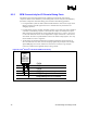
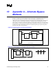
If the customer is sure that bypassed agents in the scan chain will always be depopulated, a three-
pin header bypass scheme will be adequate. As long as the bypassed agent is not on the system
board, there is no possibility of double-driving the net. Figure 23 illustrates a possible three-pin
bypass configuration. Note that when pins one and two are connected, TDO of P0 and TDO of the
ITP are connected. It is assumed that the TDO driver of P1 will not be present on this TDO net.
Figure 23. Three-pin Bypass Option
P0
TDI
TD0
TDI
TD0
P1
TDI TD0
P0 or P0,P1
2
3
1
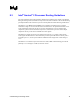
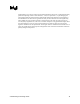
When developing bypass jumper architectures, pay close attention to how many pull-ups are
connected to a TDI/TDO net under all bypass conditions. Figure 24 shows a bypass jumper
configuration that will lead to two pull-ups on a TDI/TDO net.
Figure 24. Illegal Bypass Configuration
P0
TDI
TD0
TDI
TD0
P1
TDI TD0
P0 or P1 or P0,P1
1
2
3
JP1
P0
P1
P0,P1
2,3
1,2
OUT
JP1
Debug Port
NOTE: Note that dual pull-ups will be seen in bypass conditions. Resistance values will need to be scaled to
ensure that no less than 150 Ω is seen by ITP TDI and no less than 75 Ω is seen by ITP TDO.