
Intel Xeon Processor and Intel E7500/E7501Chipset Compatible Platform Design Guide

Intel
®
Xeon™ Processor and Intel
®
E7500/E7501 Chipset Compatible Platform Design Guide 87
Memory Interface Routing Guidelines
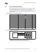
6.2 Source Synchronous Signal Group Routing
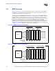
The MCH source synchronous signals are divided into groups consisting of data bits (DQ) and
check bits (CB). An associated strobe (DQS) exists for each DQ and CB group, as shown in
Table 6-3. The MCH supports both x4 and x8 devices, and the number of signals in each data group
depends on the type of devices that are populated. For example, if x4 devices are populated, the
72-bit channel is divided into 18 data groups (16 groups consisting of four data bits each, and two
groups consisting of four check bits each). One DQS is associated with each of these groups
(18 total). Likewise, if x8 devices are populated, the 72-bit channel is divided into a total of nine
data groups. In this case, only 9 of the 18 strobes are used.
NOTE:
1. In x4 configurations, the high DQS is associated with the high nibble and the low DQS is associated with the
low nibble. In x8 configurations, only the low DQS is used.
Table 6-4 states the trace length requirements for the DQ, DQS, and CB signals. All signals in a
data group must be length matched to the associated DQSs, as described in Section 12.5. Length
matching past the last DIMM connector is not critical. Route all data signals and their associated
strobes on the same layer. Try to maintain routing the signals on the same layer. If a layer transition
must occur, minimize the discontinuity in the ground reference plane. The source synchronous
signals require series termination resistors (Rs) placed close to the first DIMM connector, and
parallel termination resistors (Rtt) placed after the last DIMM connector. These solutions do not
require DQS to CMDCLK pair length matching. If you use resistor packs for the termination
resistors, it is suggested that data group signals not be mixed with Source Clocked, Chip Select, or
Clock Enable signals within the same resistor pack for validation purposes.
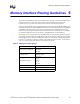
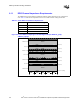
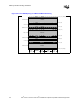
Table 6-3. DQ/CB to DQS Mapping
Data Group Associated Strobe
(1)
DQ_x[7:0] DQS_x0, DQS_x9
DQ_x[15:8] DQS_x1, DQS_x10
DQ_x[23:16] DQS_x2, DQS_x11
DQ_x[31:24] DQS_x3, DQS_x12
DQ_x[39:32] DQS_x4, DQS_x13
DQ_x[47:40] DQS_x5, DQS_x14
DQ_x[55:48] DQS_x6, DQS_x15
DQ_x[63:56] DQS_x7, DQS_x16
CB_x[7:0] DQS_x8, DQS_x17