
Dual Intel Xeon Processor Voltage Regulator Down (VRD) Design Guidelines
Dual Intel
®
Xeon™ Processor Voltage Regulator Down (VRD) Guidelines
8
2 Electrical Specifications
2.1 Output Requirements REQUIRED
2.1.1 Voltage and Current
The voltages and currents supplied by the VRD are shown in the following tables. Load-line
specifications are specified at the processor socket pins. A five-bit voltage identification (VID)
code described in Section 2.3.2 determines a reference VRD output voltage. The term "reference
voltage” indicates that the VID provides a reference point for the voltage tolerance values
provided in the Table 4. Due to voltage regulator tolerances and current draw variations, the
average voltage seen at the processor may be slightly higher or lower than the reference value.
However, VRD designers must meet the entire range of processor load and processor tolerance
limits.
2.1.2 Voltage Tolerance
Failure to meet voltage tolerance specifications at the low end results in transistors’ slowing
down and the processor’s not meeting timing specifications. Not meeting the specifications at the
high end can cause damage or reduce the life of the processor.
Unlike many previous processors, the Intel Xeon processor and Low Voltage Intel Xeon
processor specifications for V
CC
and I
CC
are interdependent. The VID definition is the absolute
maximum Vcc allowed. Icc
max
is measured at Vcc
mid
which is defined as [Vcc
max
+ Vcc
min
]/2.
The VRD regulates the Vcc voltage to:
Minimum voltage for two processors: Vcc
min
= 0.980 * VID – Icc * 0.475mΩ
Maximum voltage for two processors: Vcc
max
= VID – Icc * 0.475mΩ
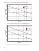
Note: These equations yield guideline voltages at the sense point. The voltage at the processor
die must meet the values specified in the respective data sheet . The voltage measured at the
sense point must be within the range shown in Figure 4 through Figure 9 and Table 2 and Table
3, except during input voltage turn-on and turn-off.
Voltage tolerance includes:
Initial DC output voltage set-point error
Component aging effects
Output ripple and noise
Full ambient temperature range and warm up
Static operation
Transient operation: dynamic output load changes from minimum-to-maximum or
maximum-to-minimum loads, as measured over a 100 MHz bandwidth.
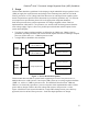
2.1.3 Output Voltage Measurements
The VRD output voltage is measured at the remote sense pins on the board: i.e., the “remote
sense connection points” in Figure 2.
Transients should be measured across the remote sense pins on the board. Use an oscilloscope
with 100MHz bandwidth, 1.5 pF maximum probe capacitance, and 1MΩ minimum impedance.
The probe’s maximum ground wire length should be less than 5mm. Ensure that external noise
from the system is not coupled into the scope probe.