
ITP700 Debug Port Design Guide


R
ITP700 Debug Port Design Guide
79
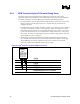
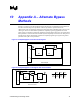
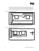
Quickswitches can be used to replace bypass jumpers/headers if the circuit is well designed. Many
quickswitch packages contain a low resistance (~7- Ω), low capacitance (~5 pF) analog bypass
switch (FET). Both the jumpers and the quickswitches designs add capacitance and resistance to
the TDI/TDO line for each device bypassed. RC delay can slow down the rise time significantly
when multiple devices are being bypassed. Careless design in this area can easily cause severe
scan frequency degradation or, even worse, scan data corruption. Using quickswitch designs allow
the system designer to actively remove agents from the scan chain by using processor present
signals as enable lines for the quickswitch. The designer must be careful to ensure that there are no
power-up conditions that will corrupt the configuration of the scan chain and therefore render this
primary debug tool inoperative.