
ITP700 Debug Port Design Guide

R
ITP700 Debug Port Design Guide 29
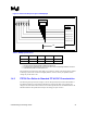
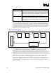
Figure 7. Recommended Bypass Jumper Configuration
1
34
2
Scan Agent 1
TDI
TDO
1
34
2
Scan Agent 2
TDI
TDO
VTAP
VTAP
VTAP
150 Ohm 150 Ohm
75 Ohm
Debug Port
Bypass
Header
Bypass
Header
TDI
TDO
When well designed, Quickswitches can be used to replace bypass jumpers/headers. System
designers should select a Quickswitch package that contains a low resistance (~7 Ω) and low
capacitance (~5 pF) analog bypass switch (FET) It should be noted that both the jumper and the
Quickswitch designs add capacitance and resistance to the TDI/TDO line for each device
bypassed. This RC delay can slow down the rise time significantly when multiple devices are
being bypassed. For example, if a design includes an analog switch of ~15 Ω of resistance and
~20 pF of capacitance used for scan chain bypass, and three scan chain agents are bypassed
simultaneously, TDI will experience an added time delay of 0.9 ns. This added delay must be
accounted for during timing analysis for recovery setup and hold of TDI under all intended
operating frequencies. Careless design in this area may result in maximum scan frequency
degradation or, even worse, scan data corruption.
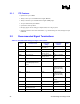
2.3.3 Execution Signal Layout Guidelines
Table 13. Execution Signal Layout Guidelines
Debug Port Signal Layout Guideline
BPM[5:0]# These signals are extremely routing critical. The debug port recovers
these signals relative to BCLK at the debug port pins. Therefore, the
signals must be routed with closely matched electrical lengths (within
±50 ps) and no greater than 1.0 ns from the closest system bus
agent to the debug port.
BPM5DR# The debug port BPM5DR# output pin should be connected on the
board to the BPM5# pin of the debug port. This allows the ITP or run-
control tool to drive BPM5# at reset. It also allows ITP to assert
BPM5# if ITP needs to assert a trigger signal that can be seen
directly by the target system. Note that ITP asserts / de-asserts this
signal asynchronous to the bus BCLK.