
Intel Xeon Processor and Intel E7500/E7501Chipset Compatible Platform Design Guide

Memory Interface Routing Guidelines
98 Intel
®
Xeon™ Processor and Intel
®
E7500/E7501 Chipset Compatible Platform Design Guide
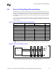
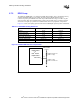
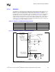
ODTCOMP, a redefined pin on the E7501 chipset MCH, is connected to the E7500 chipset MCH
DVREF_A5 pin. The E7501 chipset MCH includes active read-cycle termination for all source
synchronous signals (DQ and DQS signals). This On-Die-Termination (ODT) serves to control
signal swing at the MCH receiver during read cycles. It does not function during write cycles. The
ODT circuit has the effect of a weak pull-up of 200 Ω ± 15% to VTT. The value of termination is
not adjustable. The ODT reduces ringbacks and overshoots, and in some cases can help reduce the
need for series termination.
The E7500 chipset MCH has six VREFs per channel (12 total) while the E7501 chipset MCH only
has four VREFs per channel (eight total). The remaining four pins on the E7501 chipset MCH must
be separated from the DDRVREF plane. This can be done using 0 Ω isolation resistors between the
pins and the plane. Route DDRVREF and ODTCOMP traces 5-mil wide. When the E7500 chipset
MCH is used, the isolation resistors should be stuffed. When the E7501 chipset MCH is used, the
isolation resistors should not be stuffed. When the E7500 chipset MCH is used, do not stuff the
ODTCOMP pull-down. When the E7501 chipset MCH is used, stuff the 402 Ω pull-down.
Figure 6-16. Routing DDRVREF and ODTCOMP
Intel
®
E7500
chipset MCH
or
Intel
®
E7501
chipset MCH
E7501:Reserved/
E7500:DDRVREF_B5
E7501:Reserved/
E7500:DDRVREF_B4
DDRVREF_B3
DDRVREF_B2
DDRVREF_B1
DDRVREF_B0
E7500: no pop
E7501: 402 Ω
Ω Ω
Ω ± 1%
E7500: 0 Ω
ΩΩ
Ω
E7501: no pop
E7500: 0 Ω
ΩΩ
Ω
E7501: no pop
DDR VREF
(1.25 V)
E7501:ODTCOMP/
E7500:DDRVREF_A5
E7501:Reserved/
E7500:DDRVREF_A4
DDRVREF_A3
DDRVREF_A2
DDRVREF_A1
DDRVREF_A0
E7500: 0 Ω
ΩΩ
Ω
E7501: no pop
E7500: 0 Ω
ΩΩ
Ω
E7501: no pop
DDR VREF
(1.25 V)