
Intel Xeon Processor and Intel E7500/E7501Chipset Compatible Platform Design Guide


Intel
®
Xeon™ Processor and Intel
®
E7500/E7501 Chipset Compatible Platform Design Guide 73
System Bus Routing Guidelines
5.4 Intel
®
Xeon™ Processor with 533 MHz System Bus
and Intel
®
Xeon™ Processor with 512-KB L2 Cache
The following sections describe the differences between the Intel Xeon processor with 512-KB L2
cache (INT-mPGA package) and Intel Xeon processor with 533 MHz system bus (FC-mPGA2
package) that require special platform design consideration. Each section also provides design
guidelines addressing how to support both processor packages.
5.4.1 Intel
®
Xeon™ Processor with 533 MHz System Bus
Identification
The Intel Xeon processor with 533 MHz system bus provides both an electrical and mechanical
method for the motherboard to identify this processor. The Intel Xeon processor with 533 MHz
system bus contains an extra pin (location AE30) compared to the Intel Xeon processor with
512-KB L2 cache. This additional pin serves as a mechanical keying mechanism to prevent the
Intel Xeon processor with 533 MHz system bus from being installed in the 603-pin socket. The
Intel Xeon processors with 533 MHz system bus are only supported in the mPGA604 socket.
Section 5.4.2 contains more details about the mPGA604 socket.
The Intel Xeon processor with 533 MHz system bus uses a signal at pin AE4 named “SMB_PRT”
that is defined as a Reserved signal on the Intel Xeon processor with 512-KB L2 cache. This signal
can be used by the motherboard logic to detect the processor type. For example, platforms with the
mPGA604 socket may implement logic that determines proper support for the different
manageability features found on the Intel Xeon processor with 512-KB L2 cache and Intel Xeon
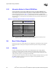
processor with 533 MHz system bus as recommended in Section 5.5. Table 5-8 summarizes the
behavior of pin AE4 on both processors.
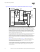
5.4.2 mPGA604 Socket
The mPGA604 socket contains an additional contact to accept the new keying pin on the Intel
Xeon processor with 533 MHz system bus package at pin location AE30 (described in
Section 5.4.1). The mPGA604 socket will also accept Intel Xeon processors with 512-KB L2
cache. Since the additional contact for pin AE30 is electrically inert, the mPGA604 socket will not
have a solder ball at this location. Therefore, the additional keying pin will not require a
motherboard via nor a surface-mount pad.
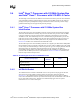
Table 5-8. Pin AE4 Signal Values Seen at mPGA604 Socket
Processor (Package Type)
Pin AE4
Definition
Output
Intel
®
Xeon™ processor with 512-KB L2 cache
(INT-mPGA package)
Reserved Z (High impedance)
Intel
®
Xeon™ processor with 533 MHz system bus
(FC-mPGA2 package)
SMB_PRT L (Grounded on package)