
ITP700 Debug Port Design Guide


R
ITP700 Debug Port Design Guide
89
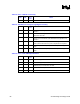
Table 45. Buffered TCK / TMS Implementation Issues
PASS FAIL Don’t’
Care
ISSUE
FBI must be used as the clock input for the buffer.
Is there an individual buffer for each TCK Load?
If there is an extra buffer in the package, FBO should be driven from that
spare buffer. Otherwise, FBO should be connected to an output of the
TCK buffer.
Can TMS be recovered at each scan chain agent given the delay of TCK
through a buffer?
Does the buffer support the drive currents and voltage regions to drive
into the pull-up on the TCK/TMS lines and match the input characteristics
of the scan chain loads?
Are TCK and TMS signals pulled LOW and High respectively through a
bias resistor to set the idle condition of the traces seen by the scan chain
agents?
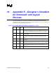
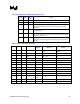
Table 46. Part 4: Pull-Up / Pull Downs
PASS FAIL N/A Signal Pin
Number
Pull Up / Pull Down
Resistance
Pull Up / Pull Down
Voltage
PWR 22 1.5 kΩ 1% for 2/3rds
recovery.
VTT of BPM[5:0]# and
RESET#
BCLK(p/n) 19, 21 See Processor Datasheet See Processor Datasheet
DBA# 4 150 – 240 Ω VCC
DBR# 6 150 – 240 Ω VCC
FBI 18 220 Ω GND
FBO 17
TCK 16 27 Ω 1% GND
TMS 12 39 Ω 1% VTAP
TDI 10 150 Ω VTAP
TDO 24 75 Ω VTAP
TRST# 14 500 – 680 Ω GND
BPM[5:0]# 13, 11, 9,
7, 5, 3,
See Processor Datasheet VTT
RESET# 15 See Processor Datasheet VTT
BPM5DR# 23 Shorted at debug port BPM[5]#